






Use of the Synopsys HAPS® FPGA-based prototyping environment
The Synopsys HAPS® System adds additional capabilities to the FPGA-based prototyping environments SoC Labs can use to support projects. The HAPS® system provides a greater amount of logic resources supporting the development of larger SoC designs. It can be used to support multiple projects simultaneously. It is used by many semiconductor companies, including ARM, for their CPU verification. This collaboration project will use the HAPS® system in SoC Labs projects and share with the community experience in utilising such systems.
A Xilinx ZCU104 ZYNQ UltraSCALE gives a capable environment for developing the nanosoc reference design. As larger reference designs are developed, they require larger FPGA-based prototyping environments to assist in their development. While a nanosoc based SoC design can be completed by a single person with a dedicated development environment, larger SoC designs require a team approach and a shared development environment. Team based development can use HAPS systems for a variety of roles in the SoC development cycle:
- verify the synthesizable RTL source code of larger SoC designs
- SoC Labs already uses a Continuous Integration and Deployment for verification approach where a virtualised environment builds the developing SoC design and regularly exercises it in a Design under Test environment. The HAPS system will improve this capability.
- support hardware/software co-design by supporting developers to write and test software on emulated SoC designs
In SoC Labs, the HAPS environment is used to support the bring-up and validation of the megaSoC reference design. This work builds on the existing use of HAPS for SoC verification and software development by introducing a structured, staged bring-up methodology that improves observability and reduces debug time.
Setting up the HAPS system
The HAPS-SX is served by a gateway machine, haps-dev, which carries the board’s USB connections (JTAG, serial consoles, SWD) and tunnels the board’s services to the development servers over a private board subnet. Nobody plugs a laptop into the chassis.
Board configuration is done in Synopsys ConfPro-SX: HapsTrak connector voltages, global clock frequencies and enables, the DDR clock, programming mode, JTAG routing and reset. SoC Labs has modified ConfPro-SX for multi-user operation; on the development server a single module load haps-dev provides it together with the programming, hardware-server, OpenOCD and board-lock commands. A WSL build is being set up so the board can also be driven from a laptop.
Programming is over Ethernet through ConfPro-SX. A VU19P bitstream (about 100 MB) loads in 20 to 60 seconds, against many minutes over JTAG. Vivado’s hardware server runs on haps-dev against the board’s physical JTAG and is used for ILA and VIO debug only.
The board is shared through a lock: haps-board-lock acquire -d <minutes> before a run, release after. A reservation always carries an expiry, so a forgotten lock cannot block the board. The HAPS-SX Development space on the SoC Labs Confluence holds the runbooks: getting started, network and command-line configuration, adding a board, HOSTIO and OpenOCD debug, ConfPro-SX on WSL, and the DDR memtest procedure.
Debugging SoC's in HAPS
The Xilinx Virtual Cable (XVC) can be used for both hardware and software debugging of the SoC being emulated in the FPGA. The software debugging is achieved by using a JTAG to AXI bridge. This takes the JTAG from the XVC into a debug wrapper. Within the debug wrapper an AXI bus can be instantiated with various debug components. Below is diagram of a basic configuration with a JTAG component, which could be connected to the Debug Access Port (DAP) of the SoC and used for software debugging, alongside an AXI-UART component that can be used to read/write to the stdio of the SoC
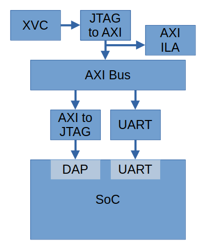
The JTAG to AXI component can be controlled using TCL commands in the vivado hardware server. A simple example of this is shown below
reset_hw_axi [get_hw_axis hw_axi_1] # reset the axi component
set address 0xC0000000
set rt axi_bram_rt
set wt axi_bram_wt

# Setup read and write transactions
create_hw_axi_txn $rt [get_hw_axis hw_axi_1] -type read -address $address -len 4
create_hw_axi_txn $wt [get_hw_axis hw_axi_1] -type write -address $address -len 4 -data {44444444_33333333_22222222_11111111}

# Write data
run_hw_axi [get_hw_axi_txns $wt]

# Read data
run_hw_axi [get_hw_axi_txns $rt]
Using this approach, tests can be written in TCL to verify the system that is instantiated in the FPGA. The System ILA can monitor the AXI transactions, an additional ILA can monitor things like GPIO from the SoC.
In addition to the JTAG-to-AXI debug wrapper described above, initial bring-up of a new design can use an Integrated Logic Analyzer (ILA) instantiated directly in the top-level RTL. This provides immediate visibility of core health signals — clock activity (via a heartbeat counter), reset release, UART transmit activity, and QSPI chip-select — over XVC, without first having to bring up the full AXI debug infrastructure. It is a lightweight first step that confirms the clock path and basic liveness before more detailed AXI-level debugging.
For designs with a Cortex-M debug port, a DAPLink on PMOD2 is served by an OpenOCD server on haps-dev, giving GDB access without the JTAG-to-AXI path; the nanoSoC DDR memtest is driven this way.
Bring-up and validation of the megaSoC reference design
The current work focuses on bringing up the megaSoC platform in a controlled and observable manner. Rather than relying immediately on full software execution, the system is validated incrementally at the hardware level.
Key integration work includes:
- Development of a top-level wrapper (haps_top) providing:
- clock distribution
- reset sequencing
- real-time clock generation
- heartbeat generation
- UART routing
- QSPI pad breakout
- Integration of the peripheral subsystem including GPIO, timers, SPI, and UART
- Validation of interrupt mapping
- Establishment of simulation-based debug infrastructure
The detailed design-flow documentation for this work, including the full pin map and the RTL adaptations, is on the megaSoC Prototyping using HAPS-SX page. The full megaSoC tape-out RTL now runs on the HAPS-SX under FPGA-only overlays (SRAM macro models, clock-gate pass-through, DRAM error slave or DDR4 wrapper, UART0 bypass). Bring-up has found and fixed several independent design defects, including a boot ROM firmware bug that would have been silent on silicon and a power-domain Q-channel tie-off that held the ROM in reset. The ROM domain now sequences and the boot ROM serves instructions to the Cortex-A53; [boot banner observed on the console / boot banner confirmation is the current step]. Detail is on the megaSoC project page (Update 10/26) and the megaSoC Prototyping using HAPS-SX design-flow page.
Debug Flow
Before generating a bitstream, the system is validated in simulation to confirm that core subsystems are operating correctly. To avoid unnecessary software debugging and ensure hardware correctness, this step-by-step process is followed:
In simulation (before bitstream generation)
- Verify clock and reset behaviour
- Confirm heartbeat and internal counter activity
- Observe CPU AXI fetch traffic
- Validate boot ROM responses and the start of the boot sequence
- Observe peripheral bus activity (GPIO/UART configuration writes)
On HAPS hardware (after ConfPro configuration and programming)
- Confirm the clock path and reset via the heartbeat (LED and/or ILA)
- Observe UART0 transmit activity
- Read boot output on the serial console, reached through haps-dev’s USB-UART on PMOD3 at 115200 baud.
- For DRAM-equipped builds, read the calibration-done bit from the DRAM wrapper’s APB status register, then run the shared memtest over OpenOCD.
Project Milestones
Do you want to view information on how to complete the work stage ""
or update the work stage for this project?
-
System Set Up
Target DateCompleted Date- Establish an initial knowledge base for the community on the HAPS system including set up requirements and other documentation
- Install the system as a network enabled service.
Result of WorkThe initial milestone to connect the HAPS as a network enabled service was completed by end of Sept 2024.
The task to establish an initial knowledge base for the community has not progressed due to other project pressures.
Our plan was to integrate the HAPS into the SoC Labs continuous integration / continuous deployment service. The next step was to deploy a SoC Labs reference design onto the platform. We achieved the later but outside of the CI/CD environment. This was to be the basis of the initial knowledge base for the community.
We will split these two tasks and close off this task.
-
Getting Started
Design FlowTarget DateCompleted DateThe guidance for the Getting Started milestone states it should help determine the best way to manage the project and to provides a simple way to manage the activities to be completed.
Project Management:
This project is not a System on Chip activity that follows the normal path of design flow steps. This project will selectively use some of the design flow steps and add some free form milestones as a way to guide the project to meet target dates to better drive the project to completion. As milestones are completed the date and details of the work need to be captured.
Design Method:
The project will use an agile method, with short development cycles, this will allow user needs to be established and then delivered. Agile usually defines a first iteration as a Minimal Viable Product.
Access to IP:
There are two aspects to this project:
- defining the IP needed from Synopsys for the HAPS operations
- defining an initial SoC design that will act as a reference model for deployment that can be used by the community as an example.
Synopsys IP:
SoC design IP:
Version Control:
Until a better alternative can be identified any materials developed by this project should be held in the SoC Labs git repository.
Project Structure:
This will need to be defined in more detail as we understand the use cases and information and other assets that need to be developed as part of the project.
The initial known outputs are:
- a knowledge base for the community on the HAPS system including set up requirements and other documentation
- a course on using HAPS as part of a real world System on Chip project.
Verification Methodology:
As outlined part of the project is to follow a typical SoC Labs reference design flow deployment using the HAPS to allow the three major uses of FPGA prototyping environments:
- verifying the synthesizable RTL source code
- integration into a Continuous Integration and Deployment service for team based projects
- support hardware/software co-design with test software on the prototype SoC design
Both MVP deliverables are defined and the first exists. The community knowledge base is the HAPS-SX Development space on the SoC Labs Confluence (getting started, network and command-line configuration, adding a board, HOSTIO and OpenOCD debug, ConfPro-SX on WSL, DDR memtest runbook). The course has not been started.
-
Set Up Project in Version Control
Target DateCompleted DateSet Up a Project in the SoC Labs Version Control.
The project is using an agile method so the the project structure will evolve. An initial project structure should allow for the initial Minimal Viable Product deliverables:
a knowledge base for the community on the HAPS system including set up requirements and other documentation
a course on using HAPS as part of a real world System on Chip project.
Board support lives in the HAPS work repository (
fpga/haps-sxbuild targets, standalone calibration designs, firmware, bench runbooks); the megaSoC FPGA target lives with the megaSoC project. -
Shared multi-user access to the HAPS-SX
Target DateThe HAPS-SX is usable by several people from the SoC Labs development servers without anyone plugging a laptop into the chassis.
Delivered: a gateway machine (haps-dev) with a private board subnet, carrying the board’s USB connections and tunnelling its services to the development servers; ConfPro-SX modified for multi-user operation and launched with a single module load alongside the programming, hardware-server, OpenOCD and board-lock commands; bitstream programming over Ethernet (a VU19P image in 20 to 60 seconds); a tunnelled Vivado hardware server per user for ILA debug; OpenOCD and serial console access through the gateway; and a board lock with an expiry so a forgotten reservation cannot block the board.
In progress: ConfPro-SX on WSL so the board can also be driven from a laptop
-
nanoSoC on the HAPS-SX
Target DateCompleted DatenanoSoC runs on the HAPS-SX as the standing bench image (the ethernet-chiplet build), proving the board, the programming path and the debug environment before megaSoC.
A DDR4 variant that reads and writes the board’s 16 GB DDR4 SODIMM through the shared megasoc_dram_wrapper is built, passes an 8 GB memtest in simulation and meets timing; its first run on the board is scheduled. It is the vehicle for proving the DDR path before the same wrapper goes into the megaSoC FPGA build.
-
Continuous Integration and Deployment for verification
Target DateAutomated build-program-test loop for designs on the HAPS-SX, built on the haps-dev infrastructure: scheduled Vivado build on the development server; automatic programming over Ethernet through haps-dev, taking the board lock; boot-banner and DDR memtest smoke tests driven through OpenOCD and the UART console; results posted back to the team.
First target is the megaSoC FPGA prototype; the same loop serves nanoSoC and the chiplet work on the same board. Tracked in Jira as MGSOC-20 (FPGA build automation) and MGSOC-23 (FPGA CI/CD flow).
Update 14/10/2026: Board access, Ethernet programming, board lock and OpenOCD/UART access are in place and used manually. The build script exists. The scheduled loop and result reporting are not yet written.
Team





 Project Creator
 John Darlington
Community lead at University of Southampton
Submitted on
Comments
Hello
Hi, our university lab has both the HAPS environment and the Zynq 104 environment. Is there anything that can contribute to this project? What is the next milestone?
Hello and FPGA use in SoC Labs
Hi,
Thank you for your message and asking about the HAPS and other FPGA environments in use within SoC Labs. We use these environments in different ways for supporting the high level design prototype activities. One difference in our use is that we have worked to make the transition from FPGA to ASIC design as simple as possible. Usually people use the hard IP blocks in the PS side of the FPGA to do a lot of the functions in the SoC design and use the programmable logic (PL side) for just their specific project design. When people move to ASIC flow they need to replicate the hard IP blocks of the PS side. Our method is to use the soft IP from the Arm Academic Access early in the design and so use more of the PL and do not depend on the PS so much.
You can find some discussion of this in the nanoSoC reference design which we utilise the Zynq 104 board as a target for design activity. We also use the FPGA environments to establish Continuous Integration and Deployment for verification of our reference designs.
We will update the milestones here and look forward to collaborating with you.
Upcoming milestons
Hi, Thanks for getting in contact.
The development of the HAPS workflow has been on pause for a little while as we're getting ready for a tape out. However the plans we have in place are to first build an FPGA image using our nanosoc reference design as this has already been implemented on the zcu104 and other zynq platforms. The main goal for this effort is to work on the debug environment for a SoC
After that the plan is to use the system for the development of an A class SoC. First will be to implement the A53 subsystem that we have already developed and again ensure that we can successfully debug this in the HAPS.
Then we will use this to further develop the A53 subsystem into a full linux capable SoC; although this is likely to take some time.
If any of these are of interest to getting involved in, please let us know
Daniel
Add new comment
To post a comment on this article, please log in to your account. New users can create an account.