Getting Started
Introduction
This Getting Started should help you to determine the best way to manage your System on Chip ("SoC") design project. One of the aims of SoC Labs is to bring industry best practice to academic led projects.
In industry there is good use of defined design and verification methods, project development environments, and specific tool chains that are re-used across many SoC design projects. Good re-use is not limited to the IP parts of the SoC hardware design but covers almost everything in the design environment, source repositories, design knowledge bases, verification environments, as well as all project deliverables including software assets and associated materials. In order to have good IP and design reuse there is a need to have investment in all the other areas of project development that support it. These are aspects that academic institutions tend not develop and even less manage to reuse across multiple projects. One of the aims of SoC Labs is share best practices across academia.
Project Management
This design flow area of the SoC Labs site lays out high level generic stages, and steps within them, that describe the necessary activities in any SoC design flow implementation.
- Architectural Design
- Behavioural Design
- Logic Design
- Physical Design
- Post Silicon
These design flows should describe the steps needed to take a System on Chip design from initial concept to final implementation. It provides descriptions on how the specific flow, tool choices and reference design implementation delivers the required system to final fabrication and post fabrication verification.
SoC Labs provides a simple way to manage the activities needed to take a SoC design from initial concept to fabrication and post silicon validation.
Once you create your SoC Labs project it is easy to add each of the activities needed to complete the project, simply 'Add new project milestone' and ...

and then select the design flow step by starting to type and select from the drop down list.

When you complete a step you can capture the date and details of the work so you can review as and when needed. It also provides help to other SoC Labs projects who can use the information to aid their projects. Here is an example from the Sensing for Precision Agriculture project by the University of Sydney.
Each of the stages and steps in the design flow area has generic information for the activity an additional information in relation to each of the SoC Labs reusable reference designs and also how the design flow step is implemented and supported within Electronic Design Automation and other design environment systems.
Look out for detail information in sections like this:
- nanoSoC reference design
Specific details on how the generic design flow step is implemented for a nanoSoC reference design
As part of your Architectural Design you will likely choose on the SoC Labs reference design platforms (nanoSoC, miliSoC, megaSoC). Look out for the section appropriate to your chosen reference design platform.
Design Methods
There are a small number of different design methodologies, our view at SoCLabs is not to be proscriptive, apart from there should be an active decision to adopt one and make best use of it for the specific design activity.
Agile Design
In this design methodology, iterating in short development cycles, each to allow additional understanding of the design purpose, is a fundamental principle.
It leads to development of a project development environment that contains Continuous Integration / Continuous Deployment infrastructure.
Formal Design
In this design methodology, additional design effort is applied to define more precisely the specification of the system such that it can be verified by formal proofs. This usually involves the use of more formal specification languages.
Access to IP
Arm supports the semiconductor industry by providing highly re-usable IP for the compute sub-system needed within a SoC design. This significantly simplifies the system development process. SoC Labs as a community uses projects to help us share and reuse hardware and software developments around core Arm IP to enable us to better achieve our research goals. A SoC Labs project is likely a selection and configuration of Arm IP to define the core of the system architecture with additional specific blocks developed uniquely as part of a project. Arm provide under the Arm Academic Access programme much of their IP to researchers for academic purposes for no charge. Its free to sign up, please ensure that you have joined the program here.
You will need to obtain permissions and download some of the Arm IP which is listed in the technology section of this SoC Labs site. The SoC Labs reference designs extend and enhance the core Arm IP tailoring it for easy adoption by the academic community. One of the first steps in Architectural Design is IP selection. which outlines some of the IP you may need to create your System on Chip.
- nanoSoC reference design
The nanoSoC reference design can utilise DMA controllers to manage the transfer of data to and from any custom accelerator. These DMA controllers need to be obtained from Arm. There are two levels of access in Arm Academic Access; the basic Foundation level and the Mainstream level. The DMA controllers are in the Mainstream level which is not the default AAA subscription. You may need to request an upgrade of your AAA subscription from Foundation level to the Mainstream level to make best use of the nanoSoC reference design.
Electronic Design Automation
EDA Tool vendors have made different choices on how to implement specific steps in the high level generic design flow stages with variations in file forms and even subtle differences in how language constructs are implemented. This means that a design that will pass verification in one tool chain may not pass verification in another tool chain. Additionally their are significant variations in warning messages across tool chains. The methods to utilise the EDA tool options and differences will be explained in sections for each tool within each generic design flow stage.
Look out for detail information in sections like this:
- Cadence
The Cadence design flow tools.
- Synopsys
The Synopsys design flow tools.
- Open Source
The open source community are also providing design support environments that simplify the SoC design task.
We encourage the community to share more examples throughout this design flow part of the site, adding material and discussions on such tool chains and example flows. You can log in and edit the pages to add material that will be moderated or simply add a comment below.
Version Control
Version Control systems such as Git are incredibly useful tools and help provide structure to project work and design activities. Having a single or multiple repositories for your project enables:
Collaboration with people able to work on different features of a project independently using branches which can then be merged, making it easy to track and visualise changes as well as see who is contributing to specific parts of a project
Delivery to others by download and use your code by cloning the repositories
Structure within your Project
There are a small number of important structures to maintain in your SoC design project and they are often hierarchical organisation schemes. For example this SoC Labs site has a hierarchical organisation scheme. How the various files in a project source control repository are structured is a hierarchical organisation scheme. How the various parts of the system design are separated and laid out usually follow a hierarchical organisation scheme.
It is important to structure the files in a project source control repository for the following reasons:
- Management of updates to reused IP - it is important to enable IP to be updated easily with minimal need to replay custom changes on top of reused IP. Keeping IP blocks in separate directories and even linked repositories which are effectively read-only and only referenced by the custom design files reduces the risk of introducing issues and your project can quickly import new version of IP patched by IP providers. It is also important when the system contains 3rd party IP which you are unable to distribute which is the case for the Arm IP.
- Project navigation - it should be easier to locate design files the designer most often needs to interact with and for those who are new to the project to quickly understand the location of source code.
- Separating significant subsystem designs from each other within the overall system design - by having subsystems (such as custom accelerators) isolated from the main system means it is easier to transfer the subsystem design into reference different systems if limitations are found in overall system performance needed to support the subsystem.
- Working collaboratively - if there are multiple people working on a project, having people working in distinct repositories can reduce conflicts within files and reduce the need to merge changes which can make projects operate a lot smoother.
- nanoSoC reference design
The repository hierarchy somewhat inverts the system design hierarchy. This was a SoC Labs design choice to hopefully make it easy to adopt for simple projects. The original release of nanoSoC was to support projects with custom acceleration hardware. The project structure is uses multiple repositories per project. The repository structure starts with an accelerator design repository soclabs/accelerator-project that contain entirely the projects custom IP files which interface to a system design top-level. The top-level system repository contains system wiring and verification material for the nanoSoC reusable design IP soclabs/nanosoc_tech
These can be forked to provide the top-level repository design files which can be customised for your project. It is worth reading project structure flow to get an idea of the suggested project structure.
The NanoSoC Tech IP repository contains the core SoC structural IP but not the IP provided via the Arm Academic Access Program (or from other IP licensing routes). The repository structure adopted for the nanoSoC reference design keeps all Arm IP in a linked repository.
See the latest nanoSoC reference design for details. Please read the README file for the git resources.
Setting up an Environment
Its important that a development environment is set up in a reproducible way such that multiple people can use the same environment and development can take place on a stable platform to prevent unpredicatble results. Using set_env scripts is one way to do this in a terminal session - it will establish environment variables which are specific to a project but will be independent of the underlying filesystem. The set_env scripts need to hook together and have no conflict if multiple sub repos are present in a project.
Verification Methodology
Verification of a SoC design uses a variety of tools and simulation models at different levels of abstraction with the overall system verified in the different design phases. At SoC Labs we invest in making as much of the verification infrastructure reusable across the different design phases. The aim is to make it easy to update and extend to add new custom subsystems and/or IP.
If you have any questions or would like to offer any views or additional information then please provide any comments or points below.
Projects Using This Design Flow

Experts and Interested People
Members


Related Project Milestones
| Project | Name | Target Date | Completed Date | Description |
|---|---|---|---|---|
| Arrhythmia Analysis Accelerator : A-Cube | Getting Started (175) |
Implement and test the Soclab encryption example in the ZCU104 FPGA board. |
||
| Sensing for Precision Agriculture | Getting Started (175) |
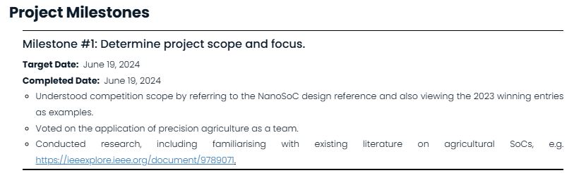
Milestone #1: Determine project scope and focus.
|
||
| Sensing for Precision Agriculture | Getting Started (175) |
|
||
| Use of the Synopsys HAPS® FPGA-based prototyping environment | Getting Started (175) |
The guidance for the Getting Started milestone states it should help determine the best way to manage the project and to provides a simple way to manage the activities to be completed. Project Management: This project is not a System on Chip activity that follows the normal path of design flow steps. This project will selectively use some of the design flow steps and add some free form milestones as a way to guide the project to meet target dates to better drive the project to completion. As milestones are completed the date and details of the work need to be captured. Design Method: The project will use an agile method, with short development cycles, this will allow user needs to be established and then delivered. Agile usually defines a first iteration as a Minimal Viable Product. Access to IP: There are two aspects to this project:
Synopsys IP: SoC design IP: Version Control: Until a better alternative can be identified any materials developed by this project should be held in the SoC Labs git repository. Project Structure: This will need to be defined in more detail as we understand the use cases and information and other assets that need to be developed as part of the project. The initial known outputs are:
Verification Methodology: As outlined part of the project is to follow a typical SoC Labs reference design flow deployment using the HAPS to allow the three major uses of FPGA prototyping environments:
|
||
| AHB eXcecute in Place (XiP) QSPI | Getting Started (175) |
Setup environment for the AHB QSPI IP |
Add new comment
To post a comment on this article, please log in to your account. New users can create an account.