nanoSoC prototyping with Xilinx(R) PYNQ(R) platform
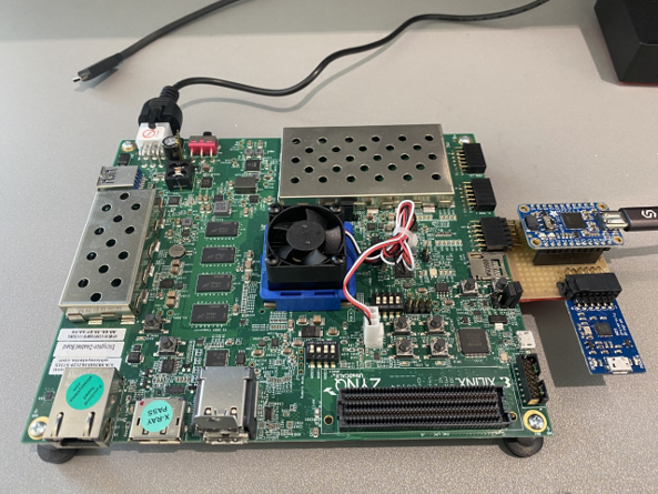
This example design flow supports the nanoSoC reference design with use of the Xilinx ZCU104 development board as a high level design prototype target. This FPGA prototyping environment has a large and capable ZYNQ UltraSCALE+ FPGA to instantiate hardware designs and Xilinx provides the Vivado tool suite for design flow execution using the board. This example design flow provides information on Xilinx Vivado software suite and how to use it for project creation, design implementation, and synthesis.
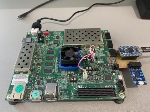
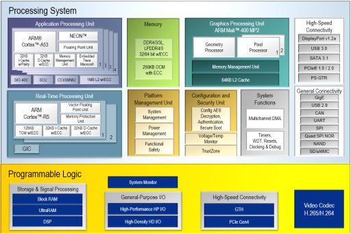
The 16nm FinFET UltraSCALE device features a Processing Subsystem with a quad-core Arm Cortex A53, dual-core Arm Cortex R5 and Mali 400 MP2 GPU. The FPGA Programmable Logic provides 504K cells which is ample resources for nanoSoC based projects. Indeed simpler, lower cost boards will support nanoSoC prototyping. The ZCU104 board is priced around $1500-2000 depending on supplier. With USB3, SATA, LPC Mezzanine, and reVISION USB HD camera connections it can support more ambitious AI and image processing research.
https://www.xilinx.com/products/boards-and-kits/zcu104.html
The PYNQ environment supports scripted control using Python of the design in the FPGA overlays of the Programmable Logic via a web-hosted server implemented on the Arm processors within the board Processing Subsystem. PYNQ supports Python software, allowing rapid prototyping in early design stages with Python libraries for data analysis and visualisation. Jupyter Notebook supports documentation and example use.
Configuring the PYNQ platform
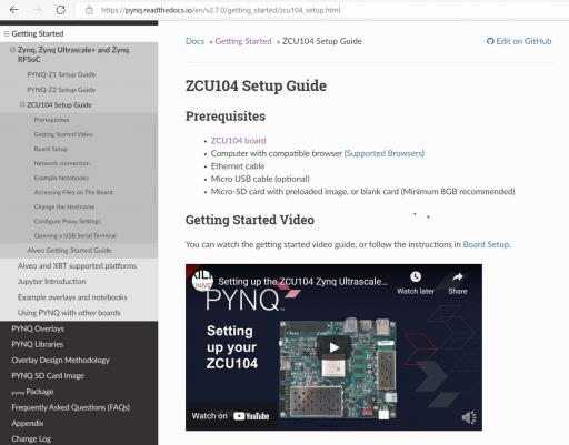
Comprehensive instructions for setting up the board are provided on the PYNQ site:
https://pynq.readthedocs.io/en/v2.7.0/getting_started/zcu104_setup.html
Follow the instructions for setting up the hostname, non-default password, and network parameters, and ensure the (re-booted) system offers network services.
Xilinx Tools
Xilinx's Vivado software suite provides a comprehensive toolset for developing FPGA designs. Version 2021.1 is available for Red Hat Linux, and you can launch it from a terminal window by typing "vivado."

Vivado launches in CLI
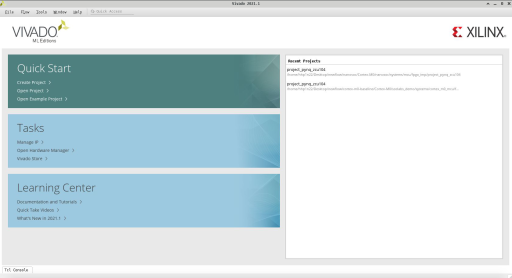
Vivado Project Launch Screen
Once you have launched Vivado, you can create a new project or open an existing one. The current project is placed under the SoC img/fpga folder.
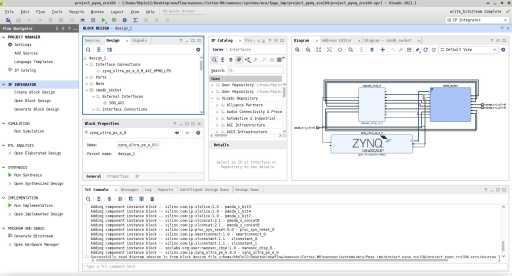
Existing project default layout
The launched project details are all visible. You can go through it and check if all board and platform details selected correctly.
Synthesis and Implementation Reports:
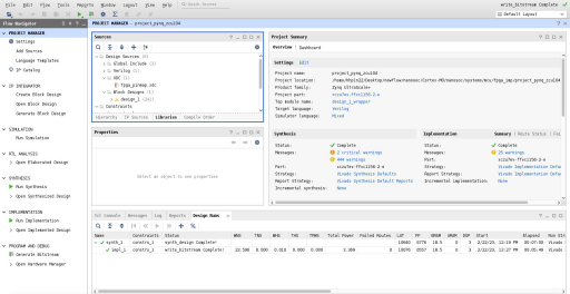
Once implementation is complete for the generated bitstream in this SoC project. Select “Open Implemented Design” in the dialog box or in the Flow Navigator on the left panel.
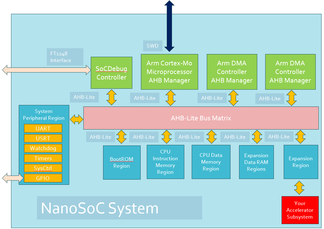
FPGA structuring for SoC test-bench
The approach adopted by SoC Labs for nanoSoC is to limit use the ZYNQ Processing System configuration to provide clocking and reset control to the SoC "Design under Test" (DUT).
The System-on-Chip design for nanoSoC is instantiated at the chip level just inside the pad-ring - to present input/output/tri-state-control unidirectional signals rather than bidirectional/tri-stated I/O-s. Care is taken to ensure that the DUT is built independent of Xilinx system IP so that the desgin can move from FPGA to ASIC flow easily. In this example flow, the microcontroller design, nanoSoC, is imported in the form of an external IP component.
The testbench "wraps" the DUT with a "socket" that is built, customized to the SoC design using the standard Xilinx Vivado "Block Design" IPXact design capture and tools, to include any specific peripherals - a UART communications channel in this case, plus generic General Purpose Input Output (GPIO) control ports to monitor or stimulate the IO ports.
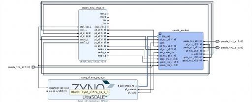
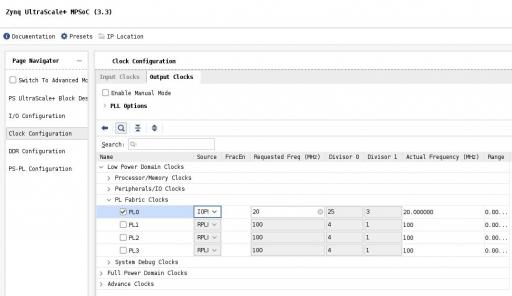
The Arm-based ZYNQ processing subsystem is completely independent of the nanoSoC DUT but provides the master clock for the device, which can be reconfigured in the Vivado editor. [Set to 20MHz for basic functional testing in the example implementation flow]
FPGA build scripts
FPGA building of nanoSoC can be done directly using the makefiles by using the command:
make build_fpga FPGA=zcu104 ACCELERATOR=yesIf you have yet to include an accelerator in the design then you can set ACCELERATOR=no
This will run through the build scripts, the exact flow can be found in the makefile.fpga file here. The steps are:
- package_socket - this packages the FPGA socket as a stand-alone IP. The socket captures communication and I/O from nanoSoC and gives an AXI subordinate to the Zynq processing system
- package_nanosoc - this packages nanoSoC as a stand-alone IP. As mentioned previously, this is done at the chip level (just below the pad level)
- build_nanosoc_design - builds the block structure shown previously, connecting the Zynq PS, socket and nanoSoc together
- output_nanosoc_design - takes the output .xsa file and unzips it to the output directory (nominally: imp/fpga/output/zcu104/overlays)
Target board specific pin map and timing constraints are accessed from the nanosoc_tech/fpga/targets/pynq_zcu104 directory
The overlay and notebook output files are copied out to the directory:
imp/fpga/output/zcu104/overlays
These files are then ready for use as Xilinx PYNQ programmable logic overlays.
FPGA programming
The PYNQ board, when successfully configured and connected to the network can be mounted as a file system and logged into from a browser.
The build scripts generate both the configuration bit-file (.bit) and hardware description (.hwh) files in the directory:
imp/fpga/output/zcu104/overlays
(default names of nanosoc_chip.bit and nanosoc_chip.hwh)
Simply copy the imp/fpga/output/zcu104/overlays sub-tree in the PYNQ board pynq/overlays/ directory
Pynq Python Scripts
You can access the pynq environment over ssh and run python scripts directly in the pynq environment.
To enable the pynq environment run:
source /etc/profile.d/pynq_venv.sh
source /etc/profile.d/xrt_setup.sh
source /etc/profile.d/boardname.sh
We have some example python scripts that are used for the nanoSoC CI/CD here
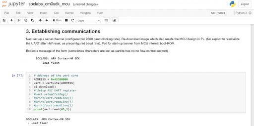
Jupyter Notebook interaction
You can also run Jupyter notebooks in the pynq environment using the instructions here: https://pynq.readthedocs.io/en/v2.7.0/getting_started/zcu104_setup.html
It should be possible to connect and log into the PYNQ server from a web browser, and select the upload any jupyter notebookts
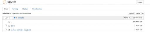
Select the ipynb notebook document and this will allow the overlay files to be loaded, checked and run to communicate with the MCU in the FPGA design (through a serial communications driver in this case):
Remote Access
SoC Labs has a Continuous Integration/Continuous Deployment service using Ian Gray’s VLAB work at York. If you would like to make it work remotely and share your resources between your team via remote server, Lance Draper has prepared an excellent guide to help you with this on VLAB.
Most research projects prefer to have in-house hands-on experience with FPGA boards. However, if you would like to join one of our requested projects in the project pages, it would be possible to set this up for you.
Projects Using This Design Flow

Experts and Interested People
Members


Related Project Milestones
| Project | Name | Target Date | Completed Date | Description |
|---|---|---|---|---|
| IMPLEMENTATION OF FIXED TIME BASED TRAFFIC LIGTH SYSTEM USING FPGA WITH VERILOG HDL. | FPGA SoC prototyping with Xilinx(R) PYNQ(R) platform (151) |
familiarize with the CAD tool. |
Initial FPGA Flow for:
Comments
This item needs a refresh based on nanoSoC tape out experience
Hi,
We should refresh this item based on nanoSoC tape out experience
FPGA Build Scripts
I have updated the link to the git repository for the SoC Labs' Example Arm Cortex-M0-based microcontroller project. This will ensure that the FPGA implementation build scripts are also synced and updated simultaneously.
FPGA Build Scripts
Hi David,
Thank you for sharing this project! I've learned a lot from your code. A few comments on the FPGA Build Scripts:
set_property top cmsdk_mcu_chip [current_fileset]
after reading in the verilog files in build_fpga_ip.tcl, and
set_property top design_1_wrapper [current_fileset]
after creating the design wrapper in build_mcu_fpga_pynq_zcu104.tcl to fix this issue.
Thank you for sharing your project!
-Meredith
FPGA Build Scripts
Hi Meredith,
Thank you for your feedback and workaround. We will address these issues and reproduce them. It's great to see it now. This exemplary project is still in development and strengthened by you and other members of our community. We hope to get it run smoother as much as possible.
Many thanks,
Hakan
Thank you so much Meredith…
Thank you so much Meredith for the detailed review feedback.
I have checked back into git the 'set_property top' fixes identified, but have struggled and failed to get to the bottom of the 'locked' IP issue you reported (which I fail to reproduce in my environment for some reason). I build up the TCL commands from running the IP packaging from the command line and despite spending a fair time digging through the Xilinx documentation have failed to find a clean alternative version. [Would you mind emailing me the journal-transcript when you next run the IPX packaging just in case this is different to what my environment gives?]
Very best wishes and do hope your FPGA prototype is making good progress
--David
IPX Error
Hey David,
I apologize for my late response. I have been working on other projects at the moment. I have tried to recreate the error with no success. The only thing I can think of- I have been running the .tcl script directly instead of the .scr. Maybe that has something to do with it. I plan on picking this project back up in a few weeks. If I run into this error, I'll be sure to document and share.
Meredith
How are things progressing
Meredith,
How is your project progressing? Did you ever find the issue re-occurred? Looking forward to hearing from you.
John.
Should this item be under the broader FPGA Prototyping topic?
Hi David,
Did you intent this item to be under this?
FPGA Prototyping | SoC Labs
FPGA prototyping design flow and example
John - thanks for reviewing this - and my premature publishing of the confusing hierarchy:
So in some ways the second is a project that refers (to and from) the Cortex-M0 reference design project and could potentially be linked to form the first as a design-flow example.
Guidance on how to repair hierarchy would be valuable: I could only think of copying to new area and then deleting the original(?)
Design Flow information structure
David,
As a community we are going to have to find our way in structuring information in ways that help us all.
The high level and generic design flow stages are traditionally described from Architectural -> Behavioural -> Logical -> Physical ...
Taking these generic flow stages and instantiating them in say a specific FPGA based flow or a specific ASIC fabrication flow and having the environment, tooling, and implementation specifics described in one place is useful.
I suggest we take some inspiration from object orientation in programming models. Perhaps this item ‘FPGA SoC prototyping with Xilinx…’ is a subclass (or derived class) of the more generic ‘FPGA prototyping’ which is a subclass of all specific design flows including for example ASIC flows.
In that case this should be a child of ‘FPGA prototyping’. You can achieve that by setting the relations in the item.
I hope this helps, John.
Design Flow information structure
We have an initial view that has the four high level generic stages of the design flow and then an area where we describe specific example flows. Hopefully we will add some more example flows to David’s initial ‘example flow’ for the Xilinx(R) PYNQ(R) platform. As we develop some additional example flows we will try and discuss how the flow delivers the requirement of the general design flow steps.
FPGA Prototyping design flows
Progress is being made to develop FPGA Prototyping design flows for the current and planned SoC Labs reference designs including determining the necessary FPGA resources required to accommodate the varying scale of the SoC Labs reference design. Flows are being developed for the initial nanoSoC design and an A class reference design. There should be more details becoming available over the next few months.
Add new comment
To post a comment on this article, please log in to your account. New users can create an account.