





Use the Tabs below to find information on community projects. Project pages have links to the 'technology' and 'design flow' stages used and ways you can comment on or join a project.
- Projects are key to community hardware design
-
As a community hardware design activity we form our collaborations around shared design actions making Projects a core of the SoC Labs community. Projects help us share and reuse hardware and software developments around core Arm IP to help us in our research goals.
- A project, takes technology and uses a design flow to make a SoC.
-
A project has a timeframe and uses the two other significant aspects of a SoC development, the selection of technology or IP blocks that make up the SoC and the design flow that is followed from specification through to final instantiation of a system. Any System On Chip usually involves the use of pre-existing IP blocks. A project team can select IP from the technology section of the site during the first stage of a design flow, Architectural Design. Later stages in the design flow support the creation of the novel aspects of the SoC design.
- Projects have a type, either active, complete (case study) or being formulated (request for collaboration)
-
Sharing information on projects much earlier than traditional academic collaboration is encouraged. Historically knowledge sharing has been at the end of the research activity, with published papers and results. As well as write up of finished projects ("case study"), ongoing projects under development ("projects") there are projects that are still being formulated ("request for collaboration") listed. We want to encourage people to engage with the project teams, for example, adding a comment to a specific project page or joining a project.
Latest Reference Design Projects
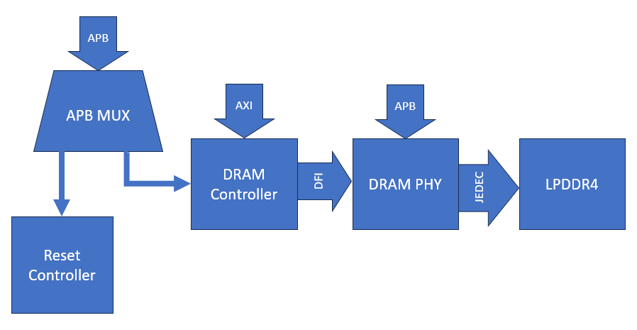
To enable full operating system support in megaSoC, a substantial amount of memory is required to accommodate the complexity of modern Linux-based software stacks, including the kernel, drivers, middleware, and user-space applications. Linux environments, unlike lightweight bare-metal systems such as nanoSoC, demand not only larger memory footprints but also consistent access to high-bandwidth memory to maintain performance across multitasking workloads. The most common approach is to incorporate external DRAM, which offers the necessary capacity and throughput.


 Daniel Newbrook
 David Mapstone
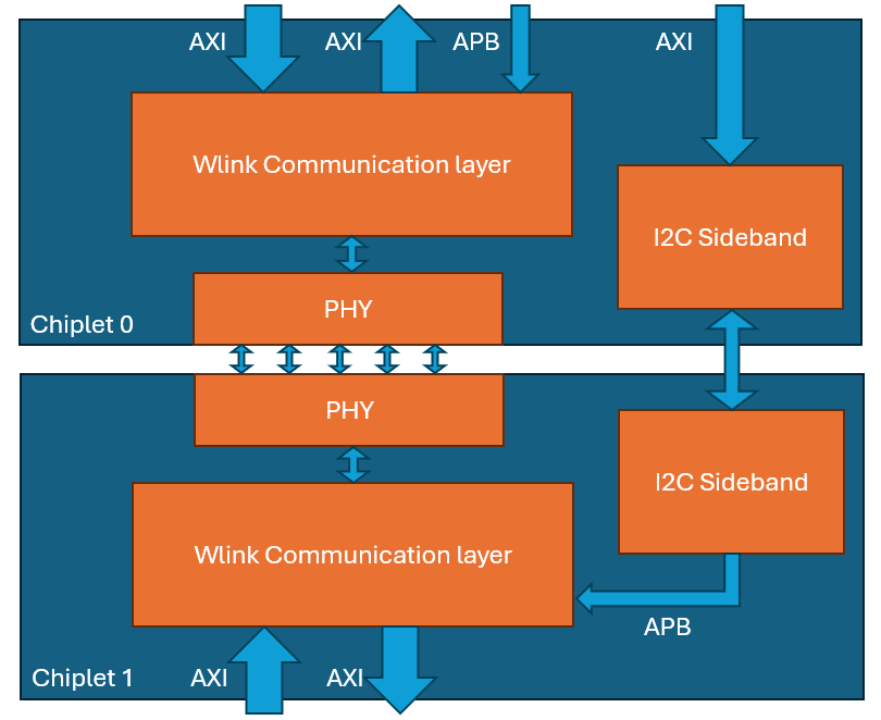
For a chiplet system, you need a communication interface between chiplets. The industry has developed standards that require complicated IPs around UCIe and the CHI interface from Arm. For many academic projects these are probably more complicated than needed . The aim of this project is to produce a simple chiplet communications interface based around the open standard AXI protocol.
The project is hosted here: https://git.soton.ac.uk/soclabs/chiplets/axi-chiplet-controller

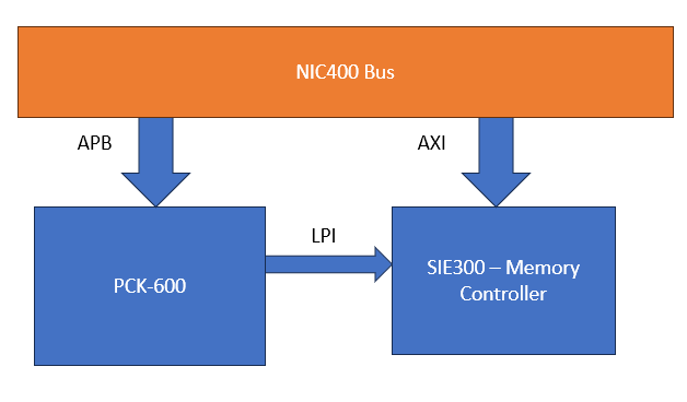
The PCK600 Arm IP provides components to allow a power control infrastructure to be distributed in a SoC in order to make a design energy efficient. Arm provide the IP as part of their Power Control System Architecture that can be used to control the power states of various parts of the system. This control of the power infrastructure is achieved through the use of the Power Policy Unit (PPU). This unit has an APB interface to allow for software control, and some low power interfaces that can connect to the power controllable IP within the system.

Latest Collaborative Projects
The goal of this project is to design and train a CNN model for spoken digit classification and deploy it on a low-cost system-on-chip (SoC) built around an ARM Cortex-M0 microcontroller with a dedicated CNN accelerator. The SoC will be deployed as a prototype on an FPGA. Its throughput, latency and energy consumption per inference, along with its FPGA resource utilisation, will then be evaluated and compared against other systems.
 Melvin Chong Qi Wen
This project focuses on the design and FPGA implementation of a low-power hardware accelerator for a Finite Impulse Response (FIR) filter, intended to reduce noise in speech signals before speech recognition. The accelerator uses a 32-tap, 16-bit serial multiply-accumulate architecture that reuses one signed multiplier and one accumulator to reduce hardware cost and energy consumption. The FIR algorithm is verified using a MATLAB model and RTL simulation.
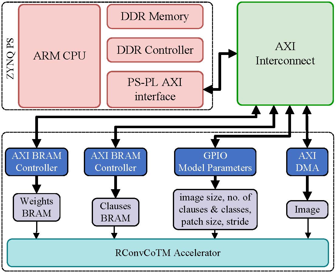
In this project, we would like to integrate our TsetlinMachine Hardware Accelerator into nanoSOC and tapeout the design.

 Srinivas Boppu
Latest Competition Projects
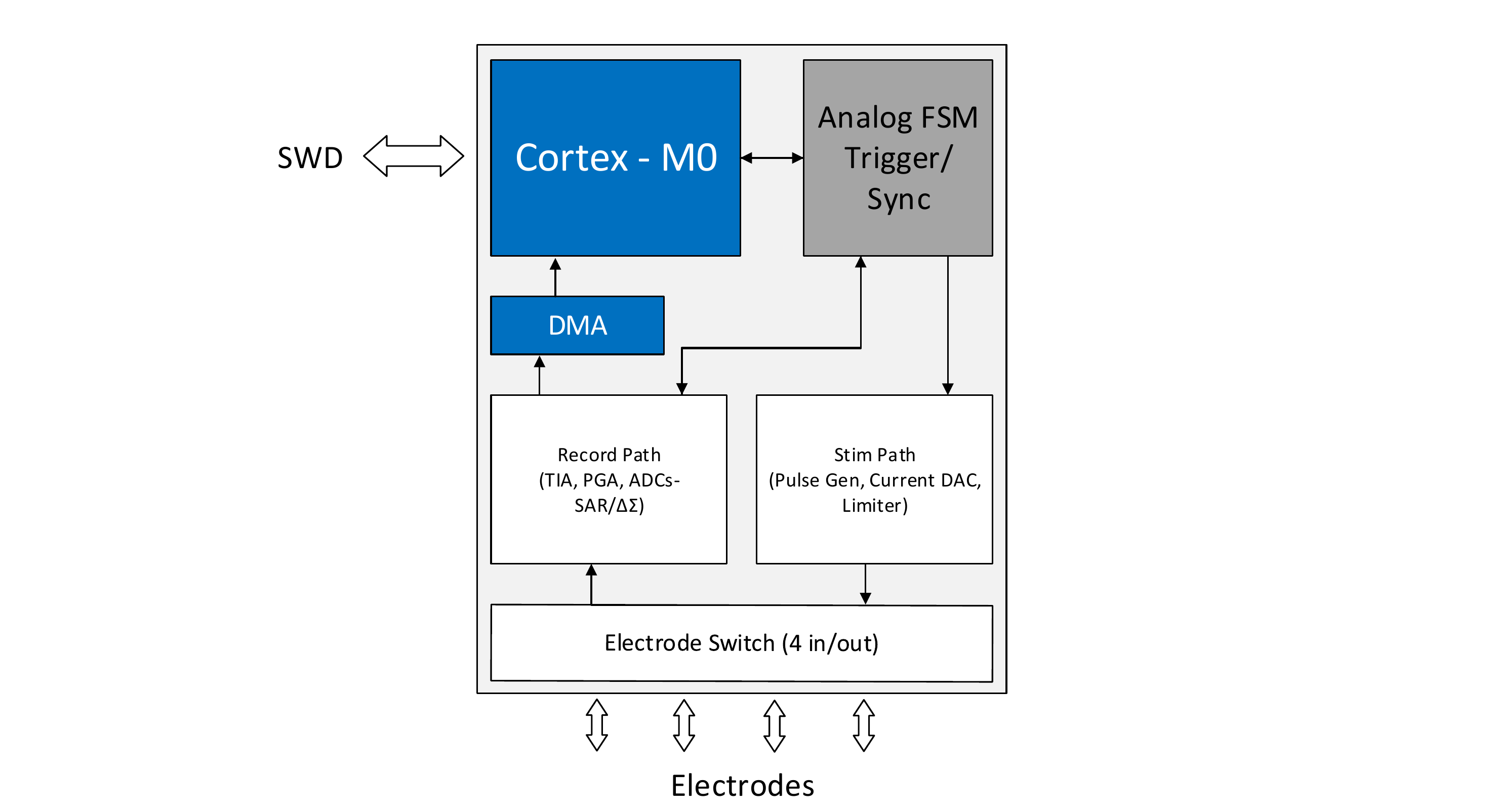
A custom chip project for recording and stimulating nerve/muscle signals, sensing an electrode's electrical activity and delivering safe, controlled electrical pulses back to it. Built around an analog front-end and dual-mode data converters for capturing both fast signal spikes and slow baseline drift, plus a closed-loop stimulation path with hardware-level safety limiting to keep delivered current within safe bounds.

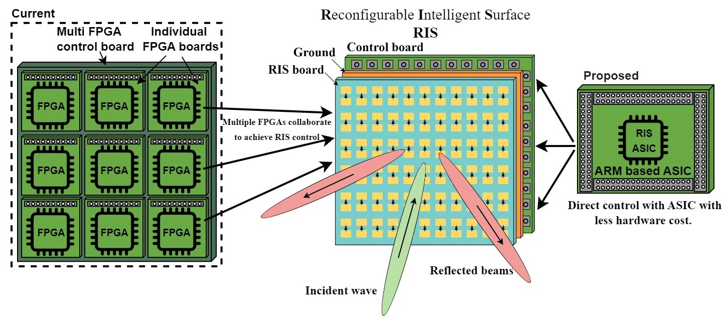
Reconfigurable Intelligent Surfaces (RIS) are planar structures composed of large arrays of tunable elements that can dynamically redirect, reflect, or shape wireless signals in the environment.
 Zhicheng Shen

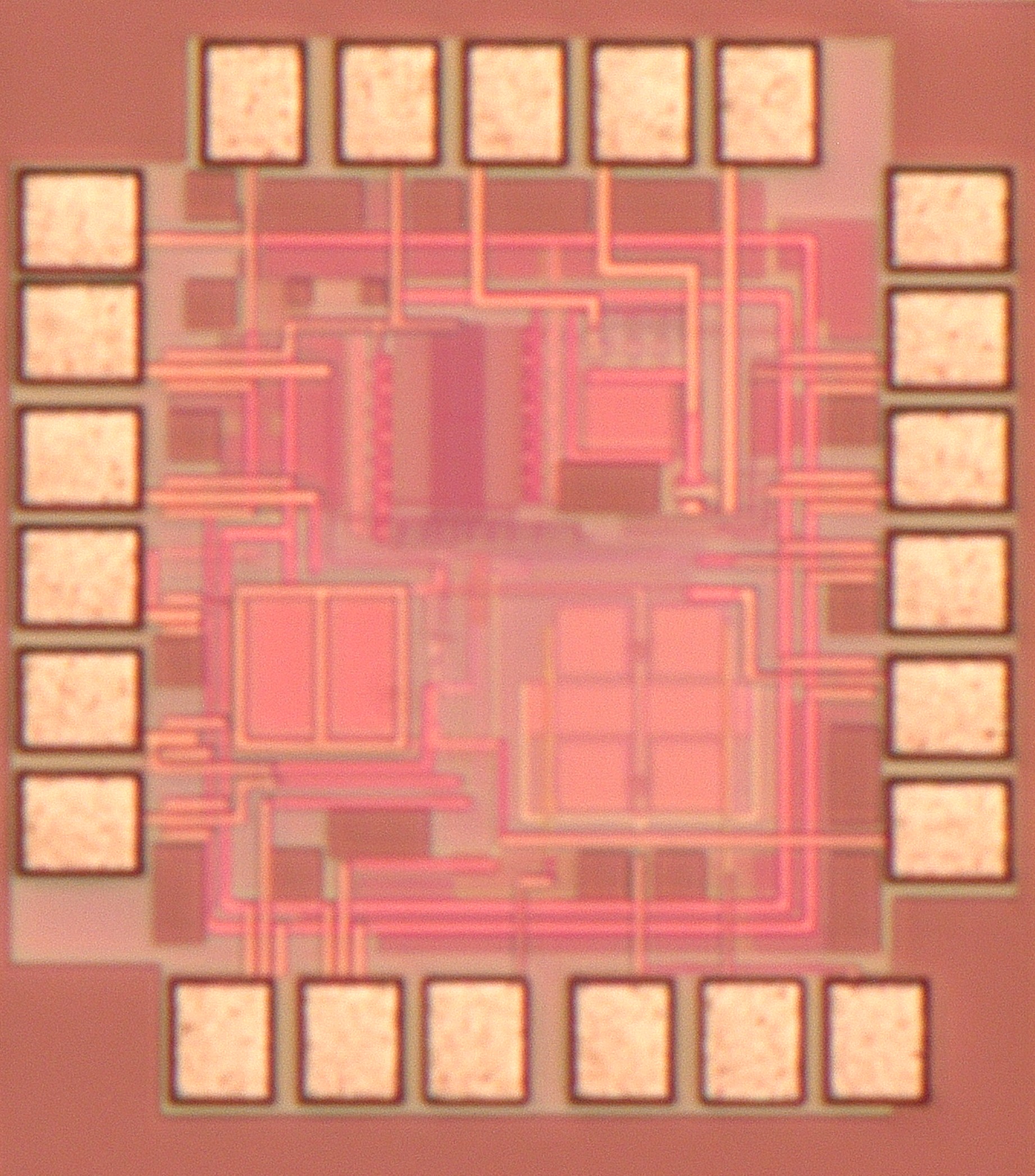
This project aims to develop an advanced RF energy harvesting (EH) receiver chip specifically designed to power embedded sensors for monitoring the condition of groceries during transportation. The receiver chip captures wireless energy transmitted from phased array antennas and converts it into electrical power that is used to operate onboard sensors, which continuously monitor critical parameters such as temperature and humidity inside delivery trucks.

 Fidel Makatia
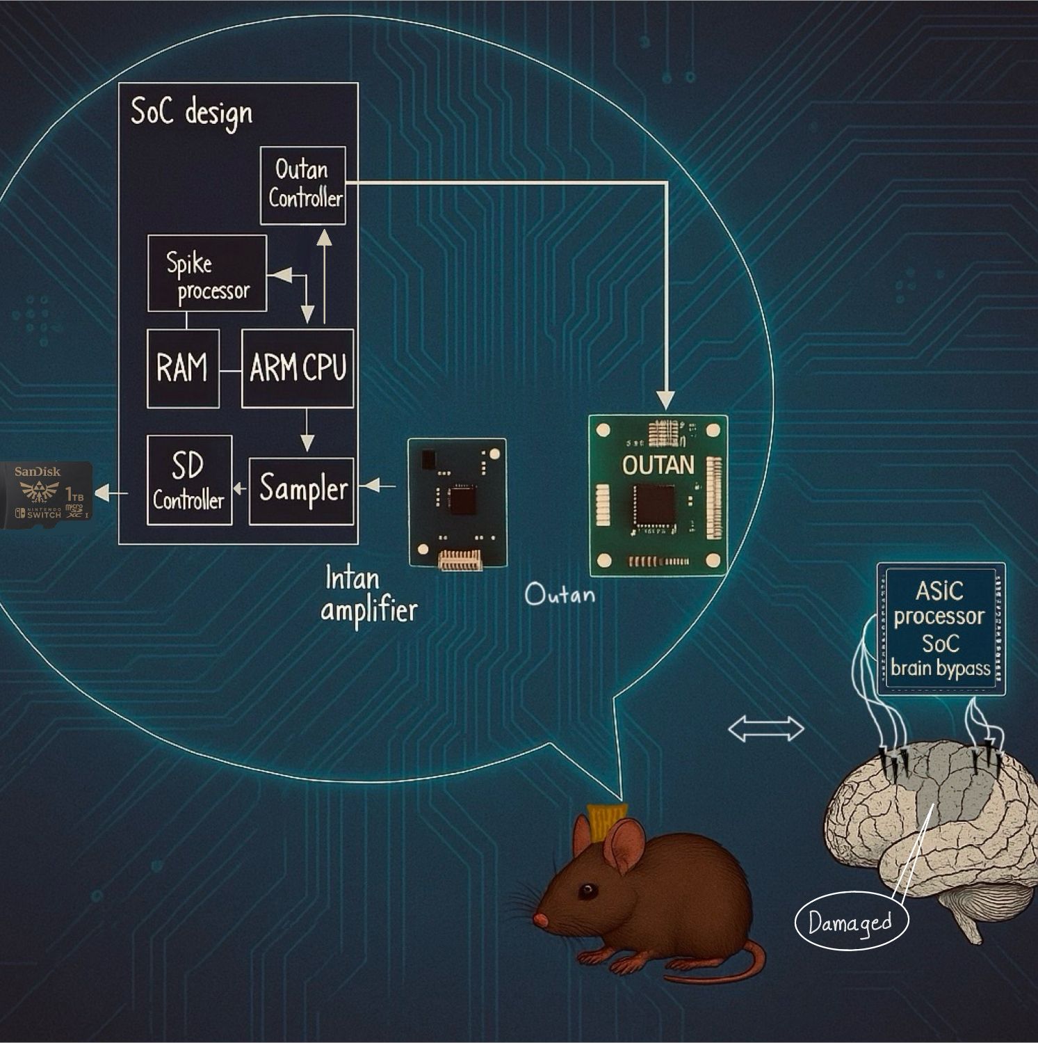
Stroke and epilepsy are among the most common debilitating neurological conditions, with a worldwide prevalence of 100 million people (World Stroke Organization, 2022) and 50 million people (World Health Organization, 2024), respectively. Present-day approaches for treating neurological and neurosurgical conditions include physiotherapy, pharmacological treatment, surgical excision, and interventions such as deep brain stimulation.




Latest Completed Project Milestones
| Project | Name | Target Date | Completed Date | Description |
|---|---|---|---|---|
| Optimized Local ML Models on nanoSoC Cortex-M0 Platform | Project Structure | |||
| Optimized Local ML Models on nanoSoC Cortex-M0 Platform | Getting Started |
|
||
| SYNAPSE — Neuromuscular Interface Chip | Project Structure |
SYNAPSE's project structure is set up following the SoC Labs accelerator-project template. The design lives in its own repo with |
||
| SYNAPSE — Neuromuscular Interface Chip | Getting Started |
A custom SoC for recording and stimulating nerve and muscle signals: it senses an electrode's electrical activity and delivers safe, controlled pulses back through the same electrodes. Built on the nanoSoC reference design with an Arm Cortex-M0. It combines an analog front-end and dual-mode data converters (fast SAR for spikes, high-resolution ΔΣ for slow baseline drift) with a stimulation path that has hardware-level current limiting. A single hardware trigger edge starts stimulation and acquisition together, giving deterministic stim-to-record timing with no software jitter. Four electrodes are shared between record and stim through a switch. |
||
| DRAM Controller integration in megaSoC | Simulation |
Simulation environment setup and working |
||
| AHB eXcecute in Place (XiP) QSPI | Routing | |||
| AHB eXcecute in Place (XiP) QSPI | Tape Out |
Target to tape this out on a TSMC 65nm miniASIC shuttle as part of the nanoSoC chiplet tapeout |
||
| AHB eXcecute in Place (XiP) QSPI | Synthesis | |||
| AHB eXcecute in Place (XiP) QSPI | Physical Verification |
DRC, LVS, ERC checking |
||
| AHB eXcecute in Place (XiP) QSPI | Clock Tree Synthesis |