Memory generators
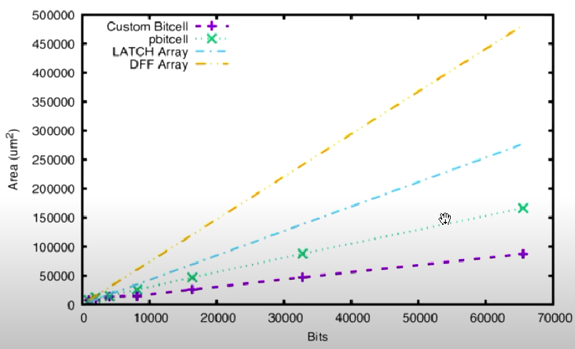
In any SoC design memory makes up a significant portion of the transistor count and area. Small memories can be synthesized using flip-flop or latch standard cells, but synthesizing large memories is inefficient in area, energy, and timing compared to using custom bits in a memory block. The cost of the circuitry (e.g., address decoders, bitline drivers, sense amps) of an SRAM memory block is quickly outweighed by the benefits of custom bit cells as memory size increases into hundreds of bits (see diagram above from Matthew Guthaus, University of California Santa Cruz).
SRAM generators or memory compilers are used to generate arrays of optimised custom bitcells in the required size of row and column configuration to best meet the needs of the SoC design. As with standard cell libraries, the SRAM generator must generate the layout and all the other EDA views for logical design, timing, power, etc.
Foundries are able optimise their custom bit cells and SRAM generators by relaxing tolerances used for standard cells based foundry specific implementation detail including lithography, materials, control of process and variation, etc. The generated memories would fail normal foundry Design Rule Checks (DRC) so are treated as a separate macro block. By taking advantage of foundry information not available externally they can minimise the dimensions of the custom bit cell while still ensuring it is robust to process variation. For this reason the SRAM generators are usually only available under specific Non-Disclosure Agreements.
Arm Artisan IP provides memory compilers for the types of memory required for a SoC design. SRAM is critical for CPU performance and used in various forms of caches. For example, the Fast Cache Instances compiler generates memory optimized for L1 cache memories. As with foundry compilers the memory blocks are highly optimized for performance, density, power and yield. Arm IP has been validated with many foundry and process technology nodes from 250nm to 3nm.
The major EDA tool vendors also provide memory compilers. As well as optimising the core custom bit cell, the significant challenge is in characterising the memory accurately taking into account their sensitivity to fabrication variation. As technology nodes get smaller the characterisation task becomes more complex, tool venders claim process variation corners(extremes of parameter variation for voltage, temperature, etc.) increase to near 200 for advanced nodes which is a complex characterisation and verification challenge and requires dedicated tooling.
The OpenRAM open source memory generator is freely available. It can be used with either custom bit cells for specific foundry nodes (it has been validated on MOSIC and SkyWater SKY130 PDKs) or using a model 45nm technology which can provide reasonable area, energy, and timing estimates (Matthew Guthaus, University of California Santa Cruz).
In summary SRAM generators take away complexity of making working and reliable memories from the SoC designer. In research scenarios however SRAM generators are not always available and either inefficient synthesis methods or open source tools such as OpenRAM allow investigation of memory challenges that may be specific to the SoC design goal.
- SKY 130
The SKY 130 has a few different options for the memory instances.
- The PDK contains some pre-built SRAM memory macros
- Some commercially available SRAMs such as from chip foundry
- Using the openRAM compiler to generate instances
Bit Density (um^2/bit) Chip Foundry ($) 5.05 Pre-built in PDK (free) 17.3 OpenRAM (free) 16.3 I suspect the OpenRAM and pre-built SRAMs are actually made from the same circuitry (I couldn't find a like-for-like comparison in terms of number of bits and the density can be affected by the actual size of the memories) but OpenRAM does give you more flexibility as it is a compiled memory instance.
Explore This Design Flow
Projects Using This Design Flow

Add new comment
To post a comment on this article, please log in to your account. New users can create an account.