Cortex-M0
The Cortex-M0 is a 32 bit processor is targeted at SoCs that require a low gate count (12-25k gates depending on configuration), small die area, high energy efficiency (0.012 mW/MHz Min Power at 50 MHz Freq, dependent on technology implementation) and is intended for microcontroller and embedded applications.
Area:
| Technology node | Die area |
| 90nm node | 0.03mm² |
| 65nm node |
The processor core implements the ARMv6-M architecture and supports In-order execution. Supports Thumb (16 bit) and subset of Thumb-2 (32/16 bit) instructions for code density / execution performance optimisation including hardware single-cycle multiply. Most instructions generated by the C compiler use the 16-bit instructions for increased code density. A simple 3-stage pipeline (fetch, decode, execute) is advanced as each instruction is executed. The register bank has sixteen 32-bit registers.
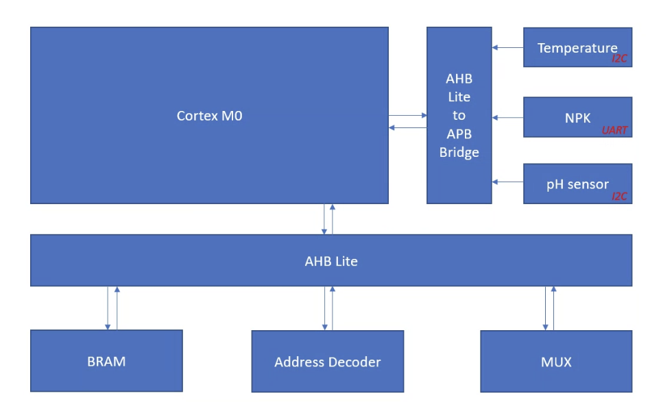
The bus mechanism (Advanced Microcontroller Bus Architecture AMBA-3) implements the AHB-lite protocol which is a simplified version of Advanced High-performance Bus (AHB) using a single master design.
The Nested Vector Interrupt Controller (NVIC) supports up to 32 interrupt inputs from peripherals each having four programmable priority levels which can be used based on the needs of the SoC design. There are additional interrupts for internal process exceptions and a Non-Maskable Interrupt (NMI) input.
Supports sleep states for ultra low-power standby to extend battery life, uses low gate count Wake-Up Interrupt Controller (WIC).
The Debug Access Port (DAP) is an optional component, defined by v5.1 of the ARM Debug interface specification. Some additional features to aid debugging ASIC fabricated devices has been added and are described in the SoC labs project for the M0 microcontroller.
Programmed fully in C, no assembler required.
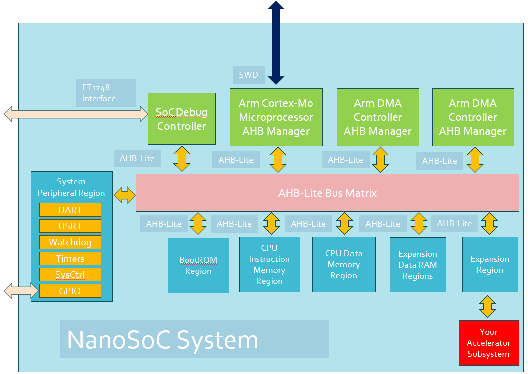
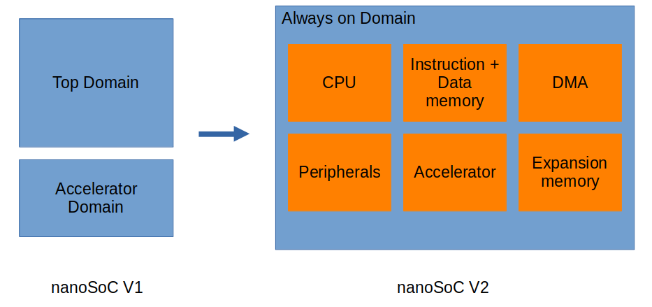
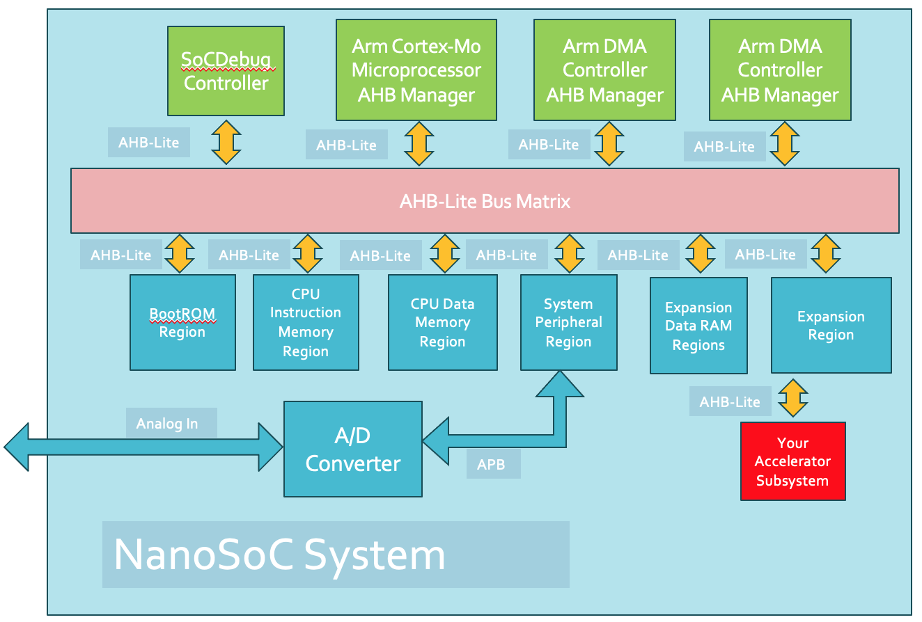
The processor is the basis of the SoC Labs entry reference design, nanoSoC, which extends the Arm pre-verified reference design to provide an easily adopted start point for an academic oriented project either for research or educational purpose. This includes provision for technology-specific mapping for either ASIC or FPGA implementation to simplify the path from FPGA prototyping to full ASIC tape out. The nanoSoC design extends the core usage case for this processor in low cost, low pin count and low power consumption scenarios.
Arm provides a few different packages to obtain the M0 IP and to integrate it into a SoC design:
- The Cortex-M System Design Kit, CMSDK, provides SoC reference designs with pre-verified IP including peripherals, documentation, synthesis scripts and software assets. It includes support for AMBA AHB designs with multiple bus masters, this allows additional masters such as DMA engines to work alongside the M0 CPU. This is the model adopted by nanoSoC to provide a simple SoC to evaluate custom accelerator designs where efficient data movement from memory is needed. It also provides a collection of peripheral IP that is the starting point for analog/mixed-signal subsystems.
- The Cortex-M0 DesignStart Eval provides a fixed configuration of the Cortex-M0 processor in a flattened and obfuscated form mainly for design and test using a simulator and hardware prototyping using an FPGA.
The SoC Labs project environment looks to support both of these ways to obtain the M0 processor IP.
Explore This Technology
Projects Using This Technology






Add new comment
To post a comment on this article, please log in to your account. New users can create an account.