
Routing
Introduction
Depending on the fabrication technology selected the number and capacity metal layers available for routing all the interconnections for a design varies making routing layout a complex 3-dimensional problem. As with other stages, design rules, routing algorithms and other layout design constraints are managed in EDA tools.
Floor planning and clock tree synthesis must be completed before undertaking routing.
There is much ongoing and historic research into how to optimise routing but it is a non-trivial. All EDA tools restrict the routing problem in terms of allowable layout of the wires, the use of vias between layers, minimising options to reduce potential for crosstalk or other radiation concerns, as well as many other design constraints. Tools are often challenged to find a compromised routing let alone an optimal routing.
In routing the layout polygons of the pins (or terminals) of the cells (circuit components in the netlist) have layout formed for the physical connections (wires) between them based on the logical connections in the netlists. The routing activity completes all the necessary interconnections between components in 2 stages, Global routing locates interconnects aiming to minimise the area used while Detailed routing aims to minimise interconnect lengths.
The use of macro blocks and consideration of the specific Input/Output needs of a design, as well as other placement decisions can have an impact of routing options. Analysis of placement density and area utilisation can allow routing to come to an acceptable layout with fewer iterations. The tighter the set of constraints on the design the more involved the potential routing issues.
Routing must ensure the design is 100% connected with no layout versus schematic violations (the layout faithfully represents the logical design) and no open or shorted paths. Signal Integrity violations can be mitigated by specifying critically sensitive nets to potential crosstalk and electromagnetic interference/compatibility concerns. This is the case for high speed, clock signal, or sensing data paths and locations close to Input/Output near the pad ring. All the metal interconnections must meet the foundry requirements, as defined in the design rule checks in the technology Process Development Kit. Design rules can vary from layer to layer. All signals paths need to meet their timing constraints. Power paths should not have any voltage or current density concerns. Many additional constraints are considered in coming to an acceptable routing that ensures fabrication and life time performance of the devices fabricated to the design.
- Cadence - Innovus
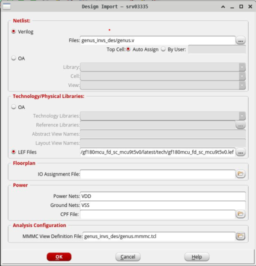
This example flow uses Cadence Innovus to route the SoC labs FT1248 to axi stream components based on the open source Global Foundries 180nm PDK.
Firstly open innovus in the common ui mode using the innovus -common_ui command. Once loaded import the design. Select the netlist from the genus_invs_des directory called genus.v. Then bring in the technology files, both the tech library which specifies the metal, via, and poly layers, as well as the library with the standard cells. This example uses the gf180mcu_5LM_1TM_9K_9t_tech.lef and gf180mcu_fd_sc_mcu9t5v0.lef files in the global foundries pdk directories. Define VDD and VSS for power and ground nets. Lastly select the generated genus.mmmc.tcl file for the analysic configuration in the genus_invs_des directory.
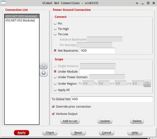
Connect the global power and ground nets to the modules power and ground nets. This can be done through the Power->Connect Global Nets ... menu
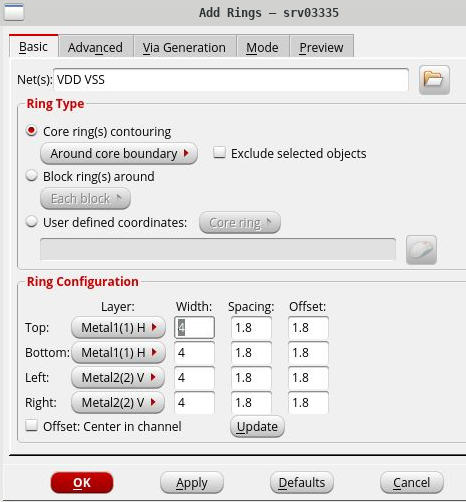
Adding power rings: go to Power -> Power Planning -> Add Ring. Add the nets VDD and VSS, and use a 4 micron wire width with 1.8 micron spacing. The metal layers these are applied to is 1 and 2, although this can be changed if necessary.
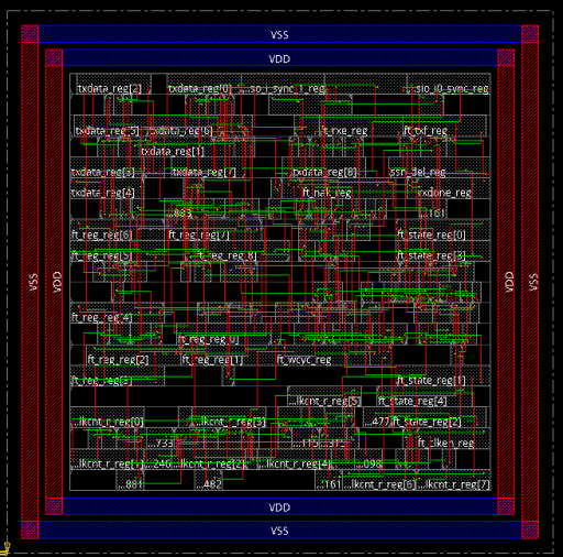
Run the initial placement: go to Place -> Place Standard Cells and make sure run full placement and include pre-place optimisation is checked.
Once this is complete, the result should be with something looking like this:
- Synopsys - IC Compiler II
Routing (route_opt command)
Projects Using This Design Flow
Experts and Interested People
Members
Related Project Milestones
| Project | Name | Target Date | Completed Date | Description |
|---|---|---|---|---|
| Aspen: A 630 FPS Real-Time Posit-Based Unified Accelerator for Extended Reality Perception Workloads | Routing (107) | |||
| megasoc re-usable SoC platform | Routing (107) | |||
| Sensing for Precision Agriculture | Routing (107) |
Comments
OpenROAD demonstration
A useful video showing the OpenROAD GUI with example use for routing congestion.
https://www.youtube.com/watch?v=wvPZREaP7E0&t=3761s
Add new comment
To post a comment on this article, please log in to your account. New users can create an account.