People
Known Good Dies
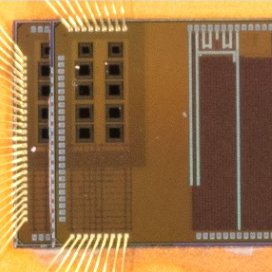
Low-cost 3D die stacking using near-field wireless communication.
This two-tier SoC, fabricated using a TSMC 65nm process, incorporates two Arm Cortex M0 CPU cores in addition to a wireless vertical AHB lite bus for inter-layer power and data transfer. The wireless AHB-Lite bus consists…
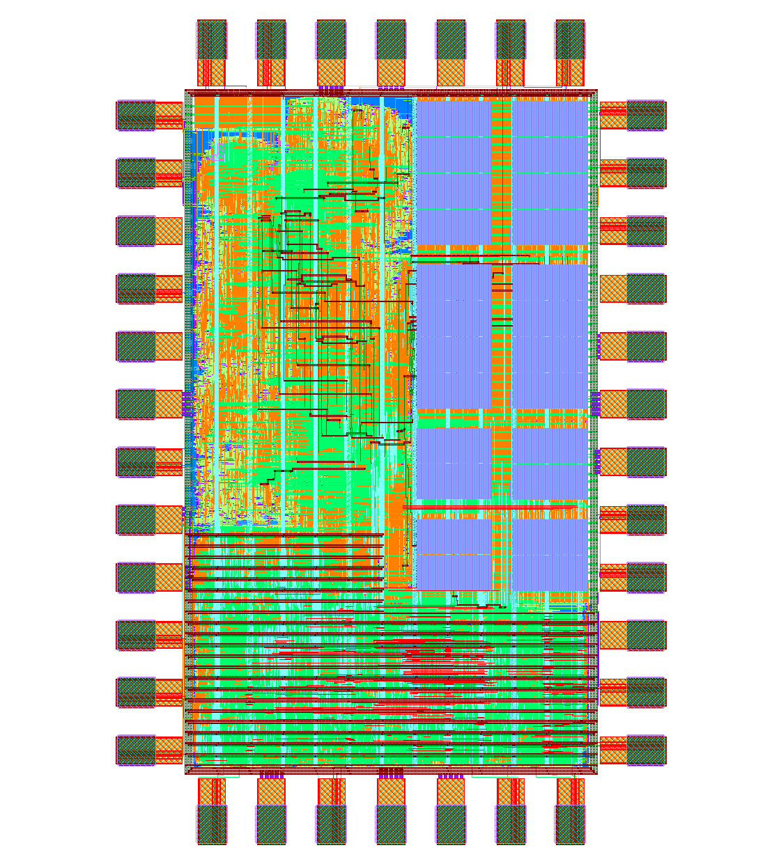
The first tape out of the nanoSoC Cortex M0 based SoC Reference Design. This reference design provides a simple microcontroller system appropriate to host and support the development and evaluation of research IP blocks or subsystems. It supports seamless transition from FPGA to physical silicon …
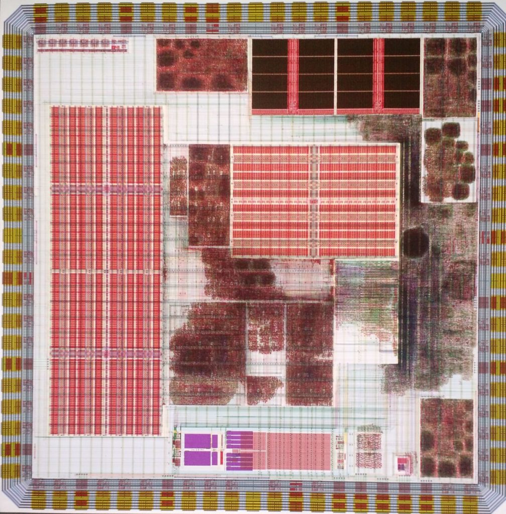
Pipistrelle-4, is the latest in a series SoCs for demonstrating multiple student projects in low-energy systems. Various circuit/system ideas from multiple researcher focusing on energy and performance with optimised SRAM bitcell and low-area overhead energy-efficient flip-flops.
P…
Projects
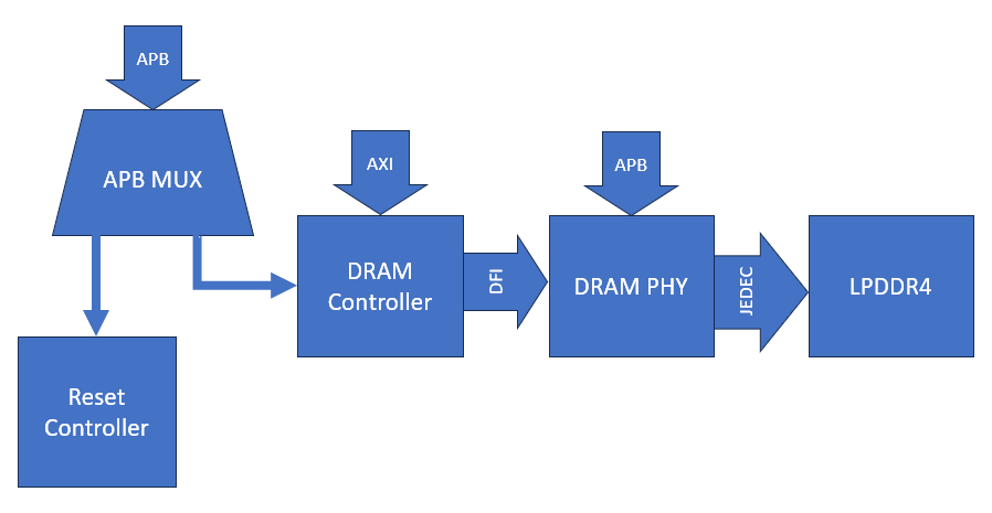
To enable full operating system support in megaSoC, a substantial amount of memory is required to accommodate the complexity of modern Linux-based software stacks, including the kernel, drivers, middleware, and user-space applications. Linux environments, unlike lightweight bare-metal systems such as nanoSoC, demand not only larger memory footprints but also consistent access to high-bandwidth memory to maintain performance across multitasking workloads. The most common approach is to incorporate external DRAM, which offers the necessary capacity and throughput.
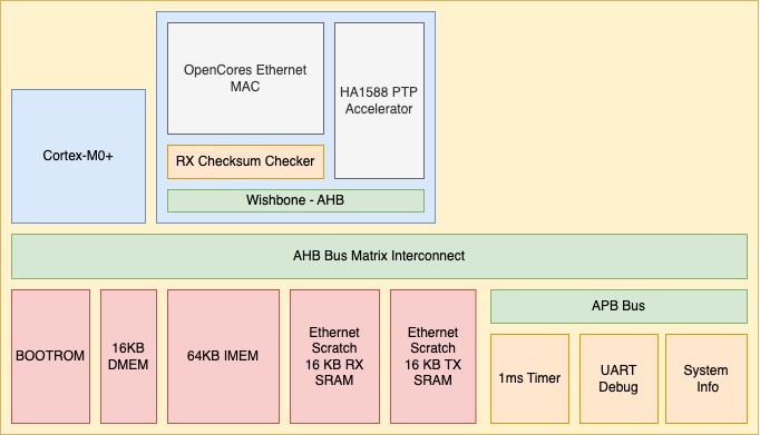
Precision timekeeping is a foundational service in any distributed system. Whether synchronising Ethernet frames to a PTP grandmaster, timestamping die-to-die packet exchanges between chiplets, or scheduling time-critical hardware events, the system needs a clock that is accurate, capturable at multiple points simultaneously, and adjustable by both hardware servo loops and software without stopping.


 Daniel Newbrook
 David Mapstone
