Technology Selection
Fabrication/deployment of a SoC requires selecting a specific technology that the independent register-transfer level (RTL) design can be transformed into a technology dependent form that can be passed to a fabrication house for manufature, deployed on a prefabricated logic such as a Field Programmable Gate Array or even just executed as a simulation.
The choice of the fabrication/deployment path for the system is based on criteria such as cost, power budget, system complexity, gate count, selected IP blocks and many other parameters.
Fabrication of devices differs by manufacturer and their specific process outcomes are described in a Foundry Process Development Kit. This is an industry standardised way to exchange details of specific technology implementation of the transistors, interconnection, etc. that can be used in Electronic Design Automation tools to design and verify the SoC ensuring that it can be fabricated/deployed.
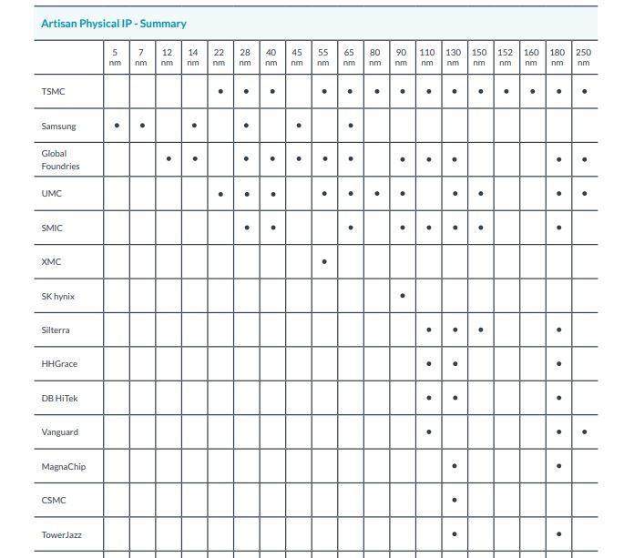
Arm works with the EDA tool vendors, foundaries and others to provide Artisan IP which they have optimized for performance of their IP for many foundry and process technology from 250nm to 3nm as shown above.
The industry has been accustomed to ever increasing transistor density in progressive technology nodes. Each node requires develoment of new lithography methods to pattern smaller features and other fabrication methods to ensure their failure free operation, the smaller features have implications on key electical and other device characteristics which affect the overall design.
Transitor and interconnect scaling was characterised by Dennard, et. al. at IBM Research. As transistor size reduces, each transistor uses less power (reduced current, voltage, electric field, capacitance, etc.) and can switch faster (increase in clock frequencies) but size also increases transister density per area so power density per area. The industry while continuing to increase transistor density has not continued to scale down voltage due to issues associated with sub-threshold leakage. Limits in gate dielectric performance and channel doping concentration issues have implications on leakage at near atomic scale. The industry has scaled down gate lengths leading to reduced capacitance and faster switching but at the expense of greater power consumption and thermal cost limiting scaling.
Interconnects, unlike transistors, do not speed up with reduced scale, the reduction in line capacitance offset by increased resistance. To improve interconnect density and circuit delay, new materials with lower resistence have been used along with low-κ dielectrics to reduce capacitance as well as adding more metal layers.
How each manufacturer deals with these fabrication challenges and the resulting device characteristics define in their unique Foundry Process Development Kit. These are usually released under non-disclosure agreements due the proprietary information contained within them. There is a growing interest in open source PDKs.
The EDA tools help the designer work through various optimisation and technology instantiation stages to transform the design between the RTL representation and the final GDSII representation needed for fabrication. The detailed characeristics in the PDK are used by the tools to ensure the design meets the rules needed to ensure fault free operation of the design post fabrication.
Standard Cell libraries help simplify the design task.
Explore This Design Flow
Projects Using This Design Flow
Related Project Milestones
| Project | Name | Target Date | Completed Date | Description |
|---|---|---|---|---|
| Sensing for Precision Agriculture | Technology Selection (111) |
Aim: Select and obtain a PDK.
Fallback: SKY130 open source PDK with Cadence MPW |
||
| nanoSoC Low Power Implementation | Technology Selection (111) |
First this project will be carried out for TSMC 65nm (as this is what nanosoc V1 was taped out using) |
||
| Aspen: A 630 FPS Real-Time Posit-Based Unified Accelerator for Extended Reality Perception Workloads | Technology Selection (111) | |||
| megasoc re-usable SoC platform | Technology Selection (111) | |||
| Arrhythmia Analysis Accelerator : A-Cube | Technology Selection (111) |
Explore technology nodes for implementation |
Add new comment
To post a comment on this article, please log in to your account. New users can create an account.