


FT1248
FT1248 offers flexibility to trade off between data bandwidth verses pin-count and can be used for a variety of off chip communication requirements.
The SoC designer can decide the width of the FT1248 data bus configuration as 1 bit, 2 bit, 4 bit or 8 bit wide depending on package constraints for pin count or data demands between the SoC and off chip fundtions. This makes for a flexible communication path versus a more traditional single serial interface or an 8 bit parallel interface.
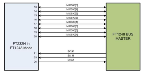
FT1248 can be configured to be a serial (with 1 data wire) interface or to have 2, 4, or 8 parallel data wires. The interface includes a clock wire (SCLK), subordinate select (SS_N) and a status line from subordinate to manager (MISO). The transfer protocol requires the manager to send a command word of 7 bits to the subordinate in n clock cycles, a single cycle for bus turnaround on the bi-directional MIOSIO wires, and then another m cycles to send the data byte. The number of cycles n and m depends on the number of wires used, for single wire this is 7 and 8 respectively, but reduces with increasing number of parrallel wires.
The nanosoc reference design uses FT1248 protocol for off chip communications to minimise pin use and to allow serial communications with the clock simply sourced from the SoC itself.
The maximum bandwidth of this interface is 30 Mbytes/s at a clock frequency of 30 MHz, but this is proportional to the number of wires used.
Explore This Technology

Add new comment
To post a comment on this article, please log in to your account. New users can create an account.