


Corstone 101 for m0/m3
Corstone subsystems integrate processors with other verified system components to form a baseline for a System on Chip ("SoC") design.
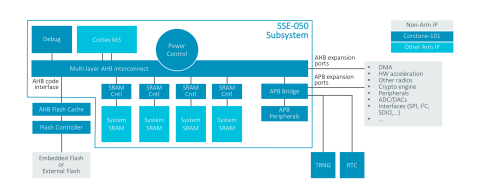
Corstone-101 is an entry level subsystem for microcontroller class processors. It is used as a baseline for SoC designs using the M0, M0+, M3 and M4 processors. Arm reference materials use the Cortex M3, with the Corstone™ SSE-050 subsystem, as their reference processor for the subsystem while SoC Labs have used the alternate Cortex M0 processor System Design Kit for the nanoSoC reference design for academia. Academia has often used the M0 processor in education and research projects making it an clear choice for nanoSoC.
Corstone-101, containing Cortex-M System Design Kit ("CMSDK"), is a package of resources including:
Components for integrating the processor with a multilayer AMBA AHB and APB bus interconnect with other IP supplied by Arm. The nanoSoC reference design uses the CMSDK IP, scripts and XML templates to generate a Bus Matrix for the SoC design.
A Joint Test Action Group ("JTAG") standard / Serial Wire Debug interface to enable debug and tracing of instructions executed in the processor. The nanoSoC reference design has adapted the Corstone-101 base to improve support for all stages of SoC development as described here.
Support for basic General Purpose Input/Output (GPIO) and Serial Communications (UARTs) peripherals. The nanoSoC reference design has a number of adaptations to the basic Corstone-101 to allow support for arbitrary SoC clock rates and remove clock dependencies.
SSE-050 has two APB based hardware timer instances to generate time events based on the system clock while allowing the processor to continue to process other instructions. The interrupts from these timers, when the counter reaches 0, are mapped to processor to signal the event. These timers are used by firmware or any operating system software running on the SoC device. Security can be enhanced by only allowing the timer memory mapped counter registers to be written to by privileged access via the operating system.
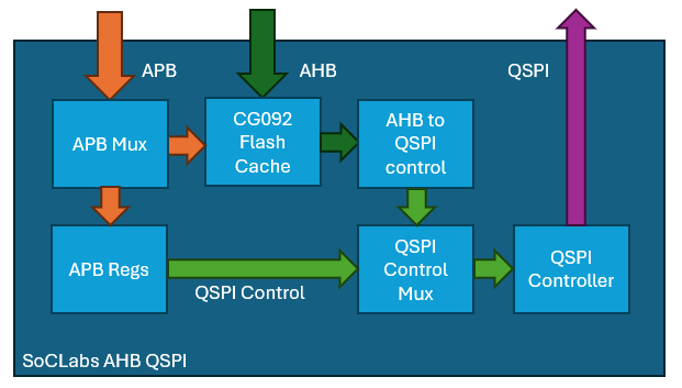
The GFC-100 Generic Flash Controller provides a way to add persistent storage to a SoC design. It allows a SoC to access eFlash memory. The flash memory controller integrates the flash memory via the Generic Flash Bus ("GFB") with Foundry IP specific components to handle the specific interfaces, timings, and protocols of the foundries memory offering. It supports an APB master interface. Communication between the system and eFlash memory is through the Generic Flash Bus.
Power management within an SoC design can be important for low power implementations especially of the device is to be powered a battery or harvested energy. The reference implementation of SSE-050 is a single power domain system. An SoC design can benefit from being partitioned into different power domains where each power domain can be managed to reduce overall system energy consumption. The SoC labs nanoSoC reference design has extended the Corstone-101 subsystem in this area by partitioning into two power domains, one for the core SSE-050 subsystem including the processor and one for the part of the SoC design associated with the academic project specific subsystem. The reason for this is not only energy efficiency but also to attain power statistics closely associated with the academic design. nanoSoC is not intended to be a complete power aware design but does provide an entry into design for power control and management.
Explore This Technology
Projects Using This Technology

Experts and Interested People
Members


Add new comment
To post a comment on this article, please log in to your account. New users can create an account.