Reference Design
Active Project
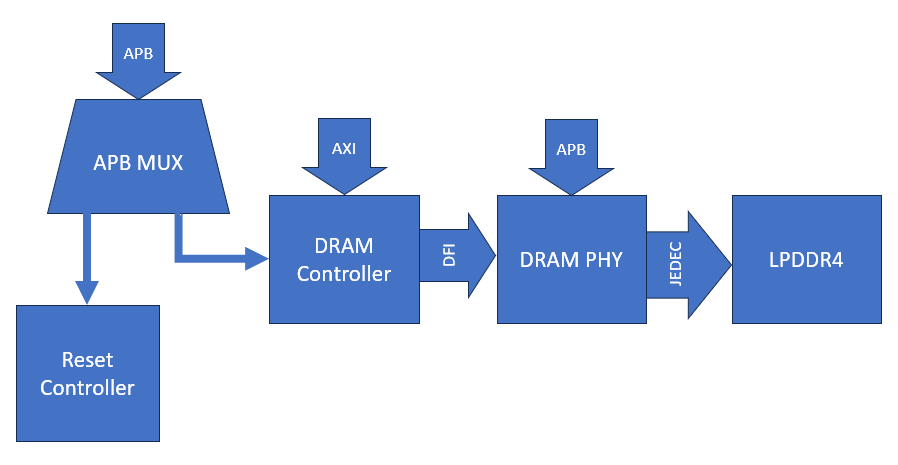
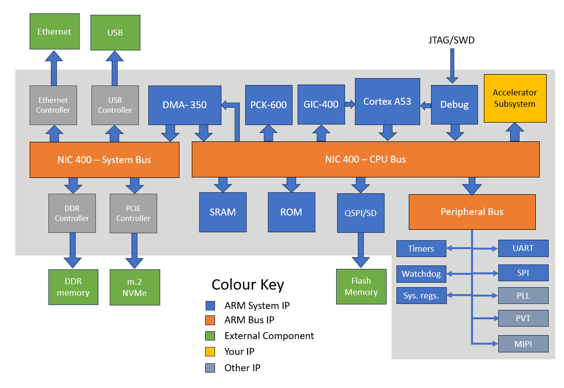
To enable full operating system support in megaSoC, a substantial amount of memory is required to accommodate the complexity of modern Linux-based software stacks, including the kernel, drivers, middleware, and user-space applications. Linux environments, unlike lightweight bare-metal systems such as nanoSoC, demand not only larger memory footprints but also consistent access to high-bandwidth memory to maintain performance across multitasking workloads. The most common approach is to incorporate external DRAM, which offers the necessary capacity and throughput.

 Daniel Newbrook
 David Mapstone
 David Flynn