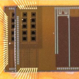
An integration of three axis accelerometers, readout circuits, an Analog to Dicigtal Convertor ("ADC") with an ARM Cotext M0 processor and memory into a single chip. The system contains algorithm calibration of the sensor and was fabrication using a CMOS MEMS platform.

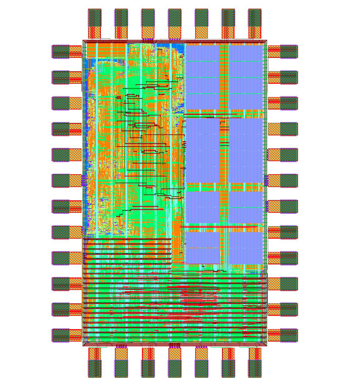
The first tape out of the nanoSoC Cortex M0 based SoC Reference Design. This reference design provides a simple microcontroller system appropriate to host and support the development and evaluation of research IP blocks or subsystems. It supports seamless transition from FPGA to physical silicon implementation utilising a memory-mapped experimental hardware subsystem.
The SoC uses a M0 core with 2 PLLs, 3 LDOs, 16KB SRAM, and 2 temperature sensors and was fabricated to aid in the evaluation of a mixed-signal SoC design framework with a number of analog block generators. It uses the AMBA™ APB protocol as the register interface to all blocks.
The temperature sensor has an area of 2,620µm2 . A 2-pt calibration is performed at 0°C and 80°C. Measured results show a sensing range between -20°C and 100°C with an accuracy of ±4°C. The generated SRAM has an area of 0.68mm2 and a custom bitcell area of 0.4mm2 .
A 3D integrated sensor system with an M3 microprocessor powered by solar cells with battery storage. It operates near threshold at 73kHz with the Wake-Up Interrupt Controller only bringing the core out of ultra-low leakage mode to take the necessary sensor readings. The system uses power gating and voltage scaling as well as custom SRAM was developed to minimize leakage power during sleep mode.
A 25mm2 SoC in 16nm FinFET technology targeting flexible acceleration of compute intensive kernels in DNN, DSP and security algorithms. The SoC includes an always-on sub-system, a dual-core Arm A53 CPU cluster, an embedded FPGA array, and a quad-core cache-coherent accelerator cluster.

Low-cost 3D die stacking using near-field wireless communication.
This two-tier SoC, fabricated using a TSMC 65nm process, incorporates two Arm Cortex M0 CPU cores in addition to a wireless vertical AHB lite bus for inter-layer power and data transfer. The wireless AHB-Lite bus consists of four, 250um diameter, inductive channels to simultaneously transmit data (at speeds up to 6Gbps) and wirelessly transfer power, whilst also allowing ‘plug-and-play’ integration with existing SoC AHB-Lite peripherals.

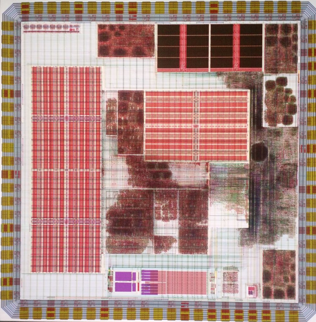
Pipistrelle-4, is the latest in a series SoCs for demonstrating multiple student projects in low-energy systems. Various circuit/system ideas from multiple researcher focusing on energy and performance with optimised SRAM bitcell and low-area overhead energy-efficient flip-flops.
Previous chips in this series include;


