Basic System Accelerator Integration Verification
A large part of the behavioural design phase of a project is actually the verification of the design at multiple levels of abstraction. This ideally involves a significant amount of verification at the accelerator internal component level (unit testing), the accelerator engine as a whole, the accelerator at the wrapper level and then system tests.
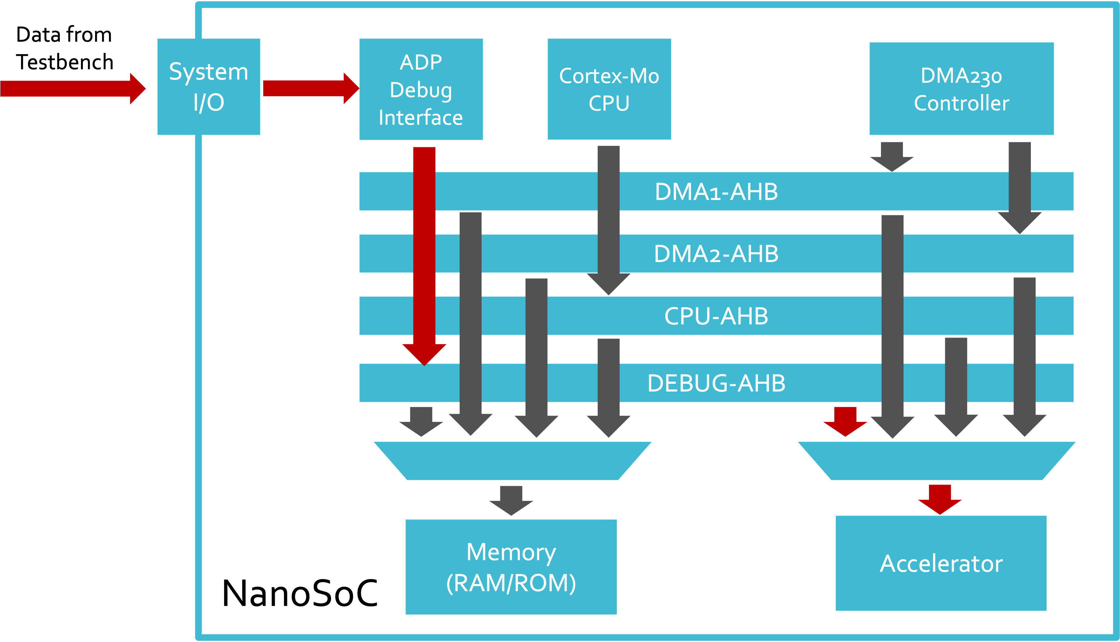
Once an accelerator has been designed and unit tested, it is then a crucial step to integrate it into a system and then verify that it has been connected correctly and is able to communicate with other devices within the system. In a system such as NanoSoC, which has multiple initiators such as a Microprocessor, DMA Controller and Debug port, it is important that these are actually able to communicate over AHB (and other interfaces if implemented) to the accelerator.
As an example, the hashing unit submodule of the SHA-2 Hashing accelerator has been taken and integrated into a NanoSoC instance. From here, the next step is to use the system initiators to perform some limited verification on the accelerator to prove they are connected together.
Verification Overview
The premise of the verification is to perform simple reads and writes from the Debug Port directly to the accelerator via the AHB-Lite Bus Matrix. By writing known stimulus data to a particular address within the accelerators address-space, the accelerator will be able to process this data and then generate data at its output which can then be read by over the debug port and then externally (by a script or by the testbench) verified against reference data (generated by an Algorithmic model of the accelerator) after the fact. This reduces the complexity overhead with designing, writing, compiling and loading code to run on the CPU or DMA Controller for initial verification.
Accelerator Structure
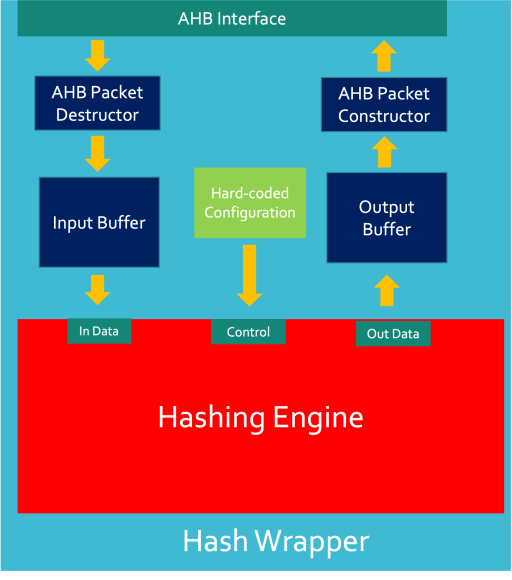
The accelerator is comprised of an AHB Interface, two packet translators – one to produce 512 bit packets to feed into the engine and one to deconstruct 256 bit packets into 32 bit AHB packets – some input/output buffers, the engine and a hard-coded configuration module to simplify implementation at this stage.
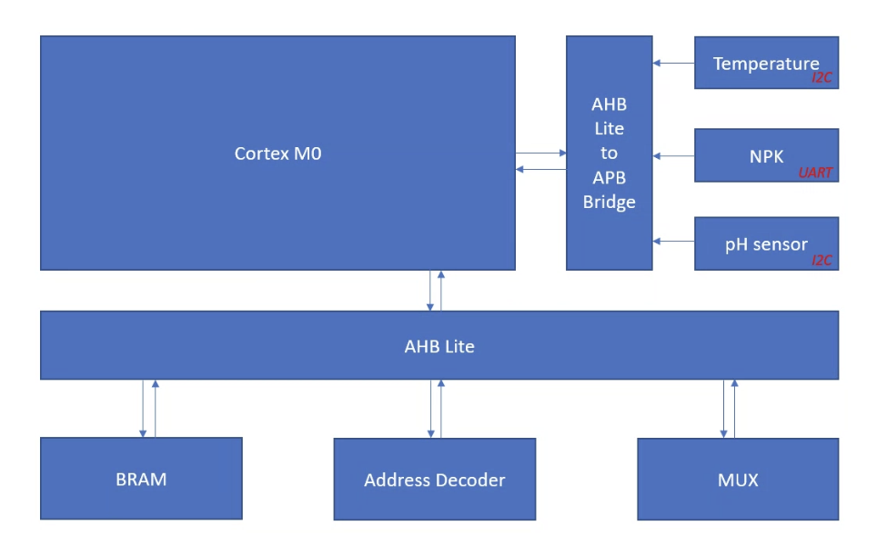
System Structure
The diagram below shows a simplified structure of our NanoSoC with AHB initiators at the top and Targets at the bottom:
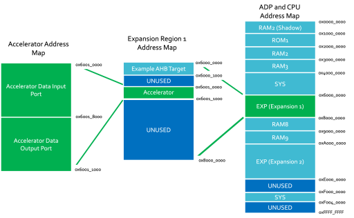
The accelerators address map will be visible to all initiators in the system in the expansion region on the global address map.
Accelerator Address Space
The accelerator will have 4KiB of address space in the first expansion region of the address map.
Verification Methodology
The first stage of verification is to make sure the accelerator is connected as specified and that it is assessable in the address map.
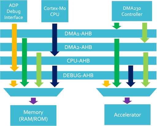
A simple verification could use a python model of the accelerator to generate 32-bit data words which can be fed into the accelerator wrapper. There are many different approaches to get the data to the accelerator but the simplest is to perform the verification outside of the system and to directly feed data into the system over the debug interface. As we are not concerned with performance at this point, we are not worried about the timing overhead compared to pre-loading the system with test stimulus.
The ADP interface can be used to write the data words to the Accelerator Input region of the address-map and then poll the output data port for a calculated response. As there are currently no registers or interfaces for the accelerator to tell the system that it has valid data, a short delay may be required between writing to and reading from the accelerator ports.

Once the data has been read from the accelerator, a simple script or part of the testbench is able to compare the read data with the expected reference data generated from the python model of the accelerator. This will be able to tell whether the verification passed or failed.
Verification Implementation
- What needed to be done to generate the stimulus?
- How was the stimulus fed into the Testbench?
- How was data verification actually performed?
Conclusion
- What should people take away from this?
- Where is most time spend?
- What is it worth having a good understanding of?
- What do these results of this verification actually mean?
- What are the next steps in System Verification?
Projects Using This Design Flow


Experts and Interested People
Members


Related Project Milestones
| Project | Name | Target Date | Completed Date | Description |
|---|---|---|---|---|
| Check year | Basic System Accelerator Integration Verification (167) |
Comments
Direction of work
Hi,
How are you getting on developing the verification flow. Do you have a direction we are headed in?
John.
Verification Flow
Hi John,
There has been a slight rethink in terms of the verification flow at different levels of hierarchy across the accelerator and system design space and I think Cocotb might be a good way to allow tests to be ported quickly at different levels of hierarchy and between different implementation platforms.
I am just trying to get familiar enough with the tools to get a good enough understanding to write an approach to component and system level verification using the tools and how exactly someone else might go about that.
I will put some additional resources together that demonstrate this clearly then come back and update this page when I have a really clear idea of how we can verify a basic accelerator in the system AND what tests we need to run - I think the second part of this is crucial as these will lay the groundwork for what other people need to get in place.
Thanks,
David M
Accelerator SoC Integration Verification
I have added the Arm reference manual where we have extracted it DDI479D and it's corresponding image of the AHB-lite interface. So they can see it when they need it.
Accelerator SoC Integration Verification
I don't think putting the detailed example wrapper in here is necessary and I will be producing my own version of the wrapper flow for others to use to wrap their accelerators up later this month. I think pointing people to the arm documentation with this information is okay, but I don't think directly copying from it is the right thing to do as we need to explicitly specify the interfaces the wrapper requires. I think putting this in here may confuse people as the ECOREVNUM signals for example aren't relevant for the Nanosoc and the detailed functionality of the example engine (the reg component in this case) is out of place. I think we just need to be careful about the information we put out regarding Nanosoc as if researchers come along and read it and then use it to spec their own accelerators off of, they may end up going in the wrong direction.
Accelerator SoC Integration Verification
One more thing, please cross link the SHA-2 accelerator page while applying these picture changes. So it can be easily accessed by curious readers :)
Accelerator SoC Integration Verification
I've just added the SHA-2 link.
Brilliant, thank you!
Brilliant, thank you!
Accelerator SoC Integration Verification
First of all, thanks for articulating it. A few things we may consider:
1)Header picture at the top would be better as an accelerator with it data in and data out representation, ahb_slave wrapper and hash engine. it's not the NanoSoC overall system picture. We can comfortably say this is our accelerator example you can swap with yours...etc.
2)Correspondingly “system structure” picture needs to be cut off as well. We don’t discuss whole system verification, accelerator is our domain only.
3)Address space is a good picture. Just it needs to be bigger. Zoom in the corresponding regions if the picture doesn’t allow you to show its text bigger by using two-three images.
4)Verification methodology picture should be again accelerator centric picture, similar the picture at the bullet point one. It needs to be drawn with an accelerator focus.
Hakan
Hi Hakan, Thanks for you…
Hi Hakan,
Thanks for you comments.
1) - I do agree but I think that the topic for the verification isn't the verification of the accelerator and the wrapper but to demonstrate we are able get data in and out of the accelerator over the Nanosoc architecture. I through this together quite quickly and I thought this was the most appropriate image I had created to demonstrate what we are trying to do in this flow - showing the data flow from outside the soc to the accelerator is what the image is trying to visualise.
I think a separate flow for wrapper verification is required to address the points you have addressed and is something that is on my to-do list when I get around to fleshing the wrapper infrastructure out further.
2) I thought the system structure picture was quite helpful to set the context for what we are trying to achieve and the fact that we have these other initiators in the system but we are deciding to only use the ADP Debug port at this time. I will probably add to this later to suggest that there are faster and (maybe better??) approaches available and how they could be carried out but our focus is clearly on using the debug interface. If you and others think that the diagram distracts from the rest of the flow, I will take it out.
3) Yeah, I agree - I can send you the full size image of this for you to use when putting the system together but unfortunately this is a technical limitation of the website at the moment. I could do as you've proposed but I think we should just push for a fix to the site instead of working around it.
4) Again back to my first point. It demonstrates how we are getting data to and from the accelerator which is the focus of this verification approach I believe.
Thanks,
David
Accelerator SoC Integration Verification
Thanks for your thoughts on this. As you said, "I think a separate flow for wrapper verification is required to address the points you have addressed and is something that is on my to-do list when I get around to fleshing the wrapper infrastructure out further."
David, at this point "wrapper verification" and "accelerator verification" are the same thing. Formal methodologies and accelerators functional verification is other topics that I am not gonna go into that rabbit hole.
My understanding is that very simple data input and output of the accelerator even trimming some control signals for simplifying it what is necessary and needed to be checked. What is the minimal data input and output for interfacing with the AHB-lite and how it looks like for this accelerator example. So it can give a glimpse of idea to other researchers how their data relation should be look like for their accelerator and dedicating a verification plan around it.
Accelerator SoC Integration Verification
Thanks for your comments.
I think we should lay out a clear distinction between engine, wrapper, system and accelerator verification. Accelerator verification encompasses all of the following and the diagram below should visualise very simply which is going on at each abstraction.
In this case, we have have missed out a stage of verification which is the Wrapper Verification which we will need to come back to as I said. The aim of this flow is for basic Accelerator "System" Verification where we are trying to verify the accelerator "through" the System Infrastructure. We are checking we have connected the accelerator (within its wrapper) into the system correctly, NOT whether the accelerator and wrapper are working correctly. We need them to work correctly in order to check the results coming back but in the case of real-world accelerator development, the verification should already be complete at both engine and wrapper level before attempting system integration - we are having to do this out of order to uncover bugs in the system integration and framework.
"What is the minimal data input and output for interfacing with the AHB-lite and how it looks like for this accelerator example" - Thank you for raising this, I will add more detail to this tomorrow in the flow but bare in mind, this is incredibly specific to the accelerator being used. A brief overview though is we will use the ADP debug port to write 16 32-bit words to the accelerator input port which will trigger a 512-bit data packet to be sent into the engine. The engine will return a 256-bit data packet which will be decomposed into 8 32-bit words which can be read back via the ADP debug port. The ADP Debug module will handle the AHB-Lite communication within the Nanosoc.
Thanks,
David
Add new comment
To post a comment on this article, please log in to your account. New users can create an account.