Collaborative
Active Project
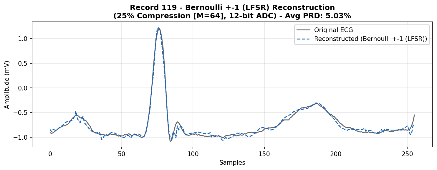
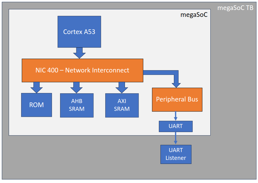
A low-power hardware accelerator for compressing Electrocardiogram (ECG) signals to extend battery life in medical devices.

 Srinivas Boppu
 Shiva Sangati
 David Mapstone


 Trio Adiono
 Daniel Newbrook