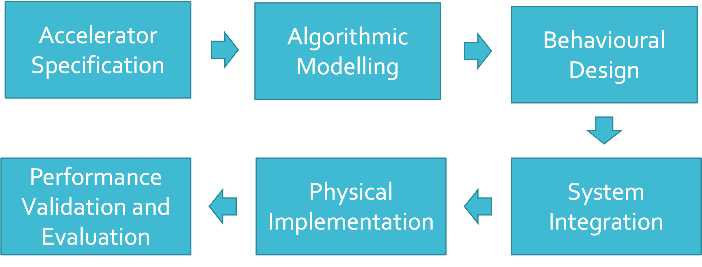
Accelerator Design Flow
Accelerator SoC Design Flow
Hardware acceleration has many advantages over dedicated software written for general-purpose processors. It can be significantly more efficient, have higher data throughput, reduce load on system resources and take up less physical space on a chip than implementing a general-purpose processor and memory - especially if the task is repetative and discrete.
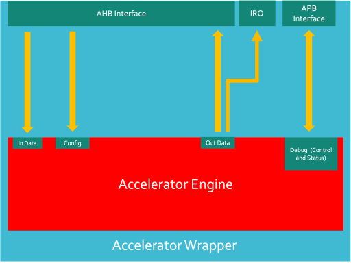
An accelerator can be made up of two main components: an engine and a wrapper. The engine is the functional part of the accelerator. This is the part of the accelerator which is performing the computation. The wrapper is an outer layer which allows an engine to communicate with a complete system.
This article is only a guide and is not prescriptive. There are many ways to go about building a hardware accelerator and integrate it into a SoC but this is the method used to build the example SHA-2 Accelerator Engine.
Prerequisites
Before building an accelerator, especially if you intend to connect it into a system, it is a good idea to do some basic architectural planning to understand how your accelerator will work within a complete system. This is basic things such as interfaces to the other logic that will be working with your accelerator, on-chip memory, throughput and system bottlenecks and debugging. In the case of the reference design for NanoSoC, most of this architectural design has already been completed and places some constraints on the design of the accelerator.
Initial Idea and Specification
Drawing up a specification for your accelerator is an incredibly important first step of the design flow. It is important to lay out the functionality of your accelerator and to specify important external requirements which may be partially dictated by the system architecture. When integrating your design into a complete system, this is crucial as you will need either conform to pre-existing requirements or dictate to others the system requirements for your design.
Important criteria to think about:
- Interfaces – bit widths of interfaces and which interfaces will need to be used.
- Input/Output Channels
- Is a single Input and Single Output channel sufficient? Would configuration channels improve data transfer efficiency if the configuration is changing at a different rate to the input data? Would multiple data input and output channels make sense in your design?
- Data throughput – how much data will be passing in and out of your accelerator.
- Will the system be able to keep up? – Will additional buffering be required on the accelerator side?
- Performance testing requirements
- How much system memory will be required to store your accelerator stimulus?
- Physical size requirements – how much area can your accelerator take up? Can your accelerator be scalable?
Algorithmic Modelling
The algorithmic modelling stage can be done in many programming languages, SystemC, MatLab and Python are all good choices but is incredibly flexible. It has two main purposes in the accelerator design:
The first is to test your idea. Does your accelerator work in the ways you initially thought? Are there modifications to your specification that you think could simplify or improve your accelerator idea? It will also give you a good idea about the data throughput and data handling on the input and output of the accelerator. Are your interfaces fit for purpose? Would it make more sense if they were designed differently.
Secondly, it is a good verification resource. If you can modify your model to generate input stimulus and output reference files, these can be used throughout the rest of the design and verification flow. If your model allows and follows a similar structure to your intended RTL model, stimulus and reference points could be created at multiple points throughout your algorithmic model which can be used for unit testing RTL modules.
Behavioural Modelling
Behavioural modelling is the point where you implement your accelerator design in your chosen Hardware Description Language, usually Verilog or VHDL.
It is important to think about your design structurally and then try and flesh out the individual components within. Take heavy consideration about the data flow within your accelerator and the points where it would make sense to separate your design into smaller subcomponents as this will help code readability, debugging and verification efforts and improve scalability.
Design techniques such as pipelining are also worth thinking about as these can improve the performance of your accelerator (after an initial overhead getting it started) but handling backpressure (how do you stall earlier stages if a later stage is stalled) can be an additional challenge. Using a Valid-Ready Handshaking system can be a good way to get around this but the interface may increase verification efforts.
Taking your RTL design, it is then important to carry out comprehensive verification to uncover bugs in your design…..
System Integration
To be able to easily test multiple accelerators on a single chip, enable improved transparency reduce IO requirements, embedding an accelerator into a system on a chip can be very effective.
NanoSoC, the SoC Infrastructure used for the SoCLabs design contest is an AHB-lite based system which has multiple Managers within such as the CPU – an Arm Cortex M0, a DMA Controller and a ASCII Debug Peripheral – ADP. These managers are connected to an AHB bus-matrix which allows each manager to have complete control over its own AHB bus. Peripherals are then connected into this bus matrix so they can be accessed by all the system managers.
The address space is broken up into several regions, most of which are assigned to various memories, however an expansion region has been reserved to allow the Managers in the system to be able to address multiple accelerators within the SoC.
To allow the accelerator to interface with the AHB expansion bus, a wrapper can be instantiated around the outside of the accelerator. The primary function of these is allow AHB writes and reads to get converted into data packets into and out of the accelerator engine. As the data width of the AHB interface is unlikely going to match that of the accelerator, multiple AHB reads and writes will need to occur to the accelerator addresses to construct packet and deconstruct packets to and from the accelerator engine.
Once the accelerator has been wrapped up, it can then be wired into the NanoSoC expansion bus where it can be addressed. This allows another abstraction for verification. The system managers can now be used to write to the accelerator with formatted stimulus and read back data which can then be compared to a reference. These are some of the ways this can be done:
- Software can be written for the CPU which can write to the accelerator and read back, performing the verification using reference data from on-chip memory.
- The DMA can be set up either by the CPU or by the ADP to perform reads and writes to the accelerator and then store the output in on-chip data memory. This memory can then be unloaded over the ADP and verified off-chip.
- The ADP can be used to directly generate AHB transactions to the accelerator – this can be done in real time or by a command script and can then be verified off chip. A basic guide of how this is accomplished for the SHA-2 Accelerator is documented here. (link)
Physical Implementation
The physical implementation can be accomplished in two independent ways - FPGA or ASIC.
Projects Using This Design Flow


Experts and Interested People
Members


Related Project Milestones
| Project | Name | Target Date | Completed Date | Description |
|---|---|---|---|---|
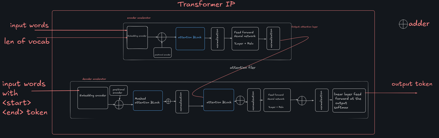
| FPGA-Powered Acceleration for NLP Tasks | Accelerator Design Flow |
implemented encoder block with hardware utilization as 22 % LUTS and 7 % BRAM. 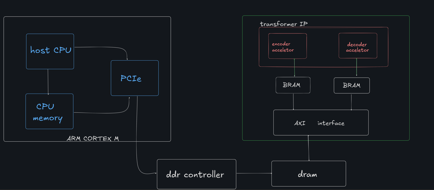
|
Add new comment
To post a comment on this article, please log in to your account. New users can create an account.