Packaging
Once a System on Chip (SoC) design has fabricated in a foundry the individual items need to be put into an electronic package that protects it from the external environment and also interconnects it to other parts of a larger system, often a Printed Circuit Board. The package may also need to perform other functions such as transfer of heat or protection from emissions that could affect device performance. One of the major design considerations is the interconnect and within the SoC design the pads that are used to make the connections to the package, traditionally via wire bonding but also via techniques using ball bonding or metal pillars.
If the design is to be combined with others as part of a Multi-Part Wafer (MPW) service then these services also usually provide a packaging service at least for standard die. As System on Chip designs become more complex advanced techniques using 3D stacking or System in Package can be used which can require unique packaging to be fabricated. A SoC may involve electrical optical, mechanical, chemical, and even biological interaction with the environment and require specific design considerations.
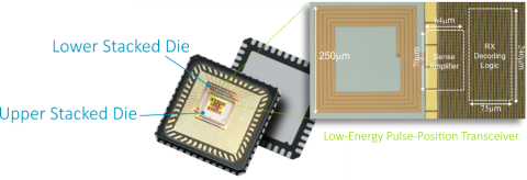
Some System on Chip designs can be implemented in a single ASIC / die. More complex designs can use advanced packaging techniques to connect several die within a package to form a system. Some designs can be fabricated at a lower cost by using multiple die than a monolithic single ASIC integration.
System Technology Co-Optimization (STCO) is a term often used to describe a design approach that partitioned the SoC into smaller modules (or chiplets) that can be designed separately and combined into larger systems in a flexible way. STCO requires the packaging considerations to be understood within the system design process including the partitioning of the various parts of the system across chiplets.
Explore This Interest
Projects Using This Interest
Experts and Interested People
Members


Add new comment
To post a comment on this article, please log in to your account. New users can create an account.