


Host-IO
Overview
Host Communications ("HOSTIO") interconnects are a class of chip-to-host computer interfaces designed to provide interactive Console communications (control, status, error and diagnostic messages) and Data transfer.
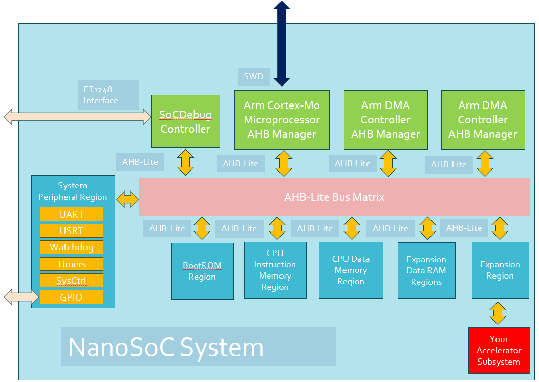
Ideally the interface to the host computer is sufficiently universal to "plug and play" with Windows, MacOS or linux drivers - or a Raspberry-Pi-based development board in the case of nanosoc silicon evaluation. USB(R) is a an ideal universal interface but complex to implement on a basic SoC, so a simpler host-io adapter can be used as the intermediate interface:
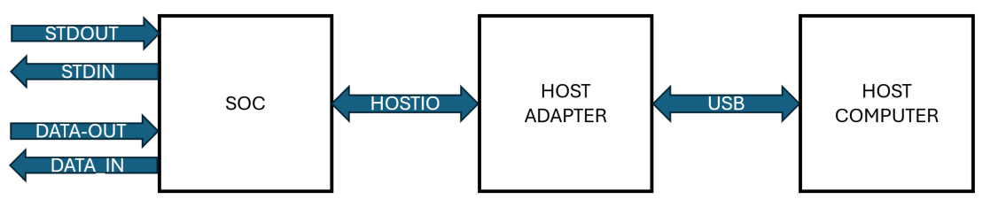
The figure shows the basic bridge between a development system-on-chip and a host computer system with a USB interface for example to provide one or more communications channels. These can be simply overlaid on a simple serial interface (such as Universal Asynchronous Receiver/Transmitter) which requires tight synchronization of 'baud' clock rates, or through more robust communications protocols that can provide 'handshake' signalling to cope with widely differing or dynamically-varying clock frequencies. This is valuable when running a SoC in low power modes with very low frequency clock or R-C (resistor-capacitor) oscillator with dynamic PLL clocked modes of operation.
Clocking options
The clocking options may be summarized as:
- Asynchronous - require synchronization information in the data and subsequent data sampling
- Source synchronous - the controller provides the clock signalling for the target timed with the data
- Phase-locked synchronous - the target is responsible for frequency and phase locking to the controller after some 'learning' scheme
- Hardware-handshaking - explicit request and acknowledge signalling between target and controller
- (Or for sophisticated SoC or FPGA design, a USB controller with PHY interface to abstract the communication interface)
Commercial Future Technologies FTDI-1248 interface
The first generation of 'nanosoc' designs implemented a bit-serial "FTDI1248" controller. The clock for this protocol is sourced from the SoC. It supported communication through a Future Technologies Devices Inc USB module that provides console character input with the chip clocking from 10's of Hz to 10's of MHz, operating with standard digital IO drivers and pads. The clock and bidirectional data transfer support and signalling is implemented using a four-wire method and offers up to megabytes of data per second communication rates.
SoC Labs HOSTIO4 interface
The second generation of nanosoc has an alternative interface to accommodate higher SoC clock frequencies, and to add support for independent bulk data transfer on- and off-chip.
Console I/O typically supports
- STDOUT 'Standard Output' character transmission to host
- STDIN 'Standard Input' character transmission from host to SoC
In the case of the nanosoc platforms, a mechanism is supported to an ASCII Debug Protocol (ADP) bare-metal debugger for code and data
- ADPOUT - ADP diagnostic and message transmission from SoC to host
ADPIN - ADP control and data transmission from host to SoC
(but these share the same underlying Console output and input channels)
USB interface controllers typically support these communications channels with FIFO buffering to improve peak transfer rates but present simple 8-bit character streams to and from the host system.
Learning from the first round of nanosoc-based research projects, support has been added for independent data-plane channels independent of the console channels
- XDO eXternal Data Output byte transmission to host
- XDI eXternal Data Input byte transmission from host to SoC
Rather than adding extra hardware pins and wires (given the pin-limited SoC pad counts and bonding) these are implemented as Virtual Channels sharing the same underlying I/O hardware.
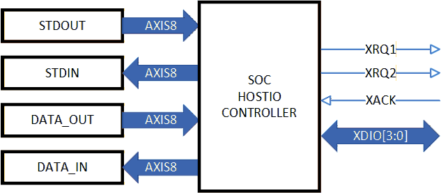
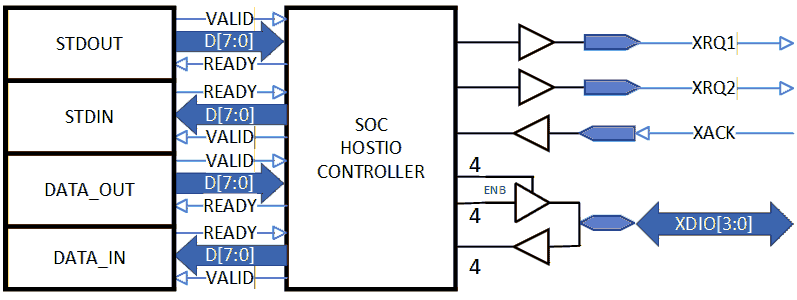
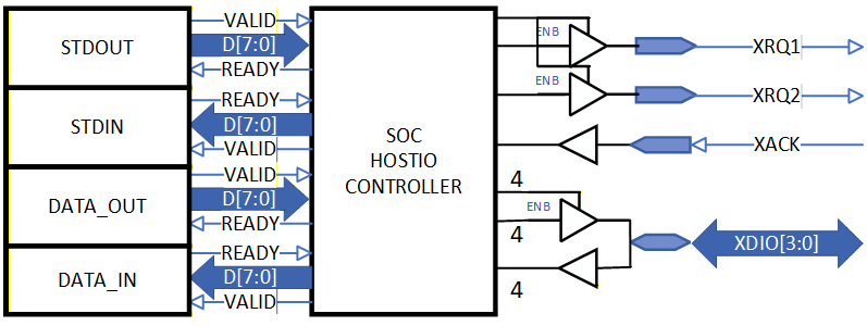
For the second generation, nanosoc-2025, this is implemented as a "HOSTIO4" implementation: supporting 4 x 8-bit virtual channels using a 4-bit data bidirectional communication data channel bundled in a 7-pin/wire interface:
- 2 transfer request signals from SoC to Host: XREQ1, XREQ2
- 1 transfer acknowledge to SoC from Host: XACK
- 4-bit bidirectional status/command/data packet transfer bus: XDIO[3:0]
To improve the design reuse in SoC designs and FPGA implementations or prototypes all the data channels are implemented as 8-bit AXI-stream interfaces. These provide hardware-handshaking transfers at the byte level.
A simple packet transfer protocol provides the sequencing of the bidirectional bus driving and safe tri-state "turnaround" slots, and synchronization registers are added on the appropriate inputs to support fully-asynchronous independent clocking of SoC and Host,-adapter, using standard SoC digital IO pads.
The Host "target" provides 'ready' status visibility for the four virtual channels implemented: RX-data-empty and TX-data buffer-full for both Console and Data channels.
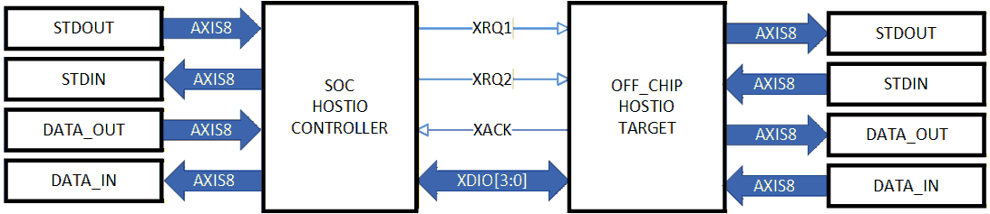
The on-chip controller initiates transfers with the host depending on which virtual channels are ready and which streams are actively requesting transfers.
The interface drives standard off-chip bidirectional Input/Output pad drivers:
Prototype Hostio4 USB interface
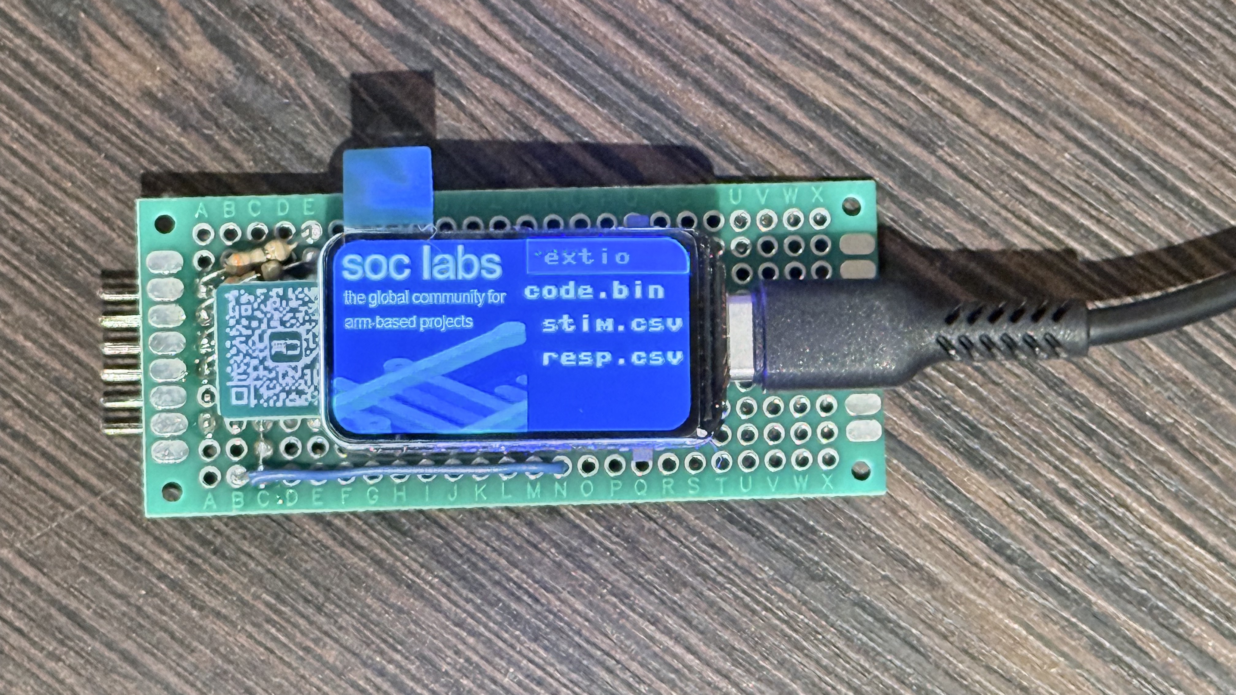
The target interface protocol can be implemented by a microcontroller as a simple bit-banged PIO port, or for more optimal communication performance can be coded efficiently to use the "PIO" state machines provided in Raspbery Pi Pico controllers. The photograph below depicts the prototype interface developed for validating the SoC interface over a PMOD interface from FPGA. Example micropython code is provided in the supporting github project (link at the end of this page).
Enhancement for communication with one of multiple chiplets
The HOSTIO4 interface was originally designed for debugging and early evaluation of test-chips with a direct (7-wire) connection. Adding in multiple parallel interfaces per-chip in a multi-chiplet project is not ideal so an extension to the interface protocol has been devised to enable a "de-selected" mode to be supported by using the system reset signalling and an independent "XACK" control handshake signal per chip.
The SoC controller state machine remains deselected from reset as long as the XACK input to that controller is held active (logic-1). Only the chiplet under active debug connection has XACK driven by the Host target protocol state machine; all other chiplets have their XACK inputs pulled-high or configured through links to VDDIO.
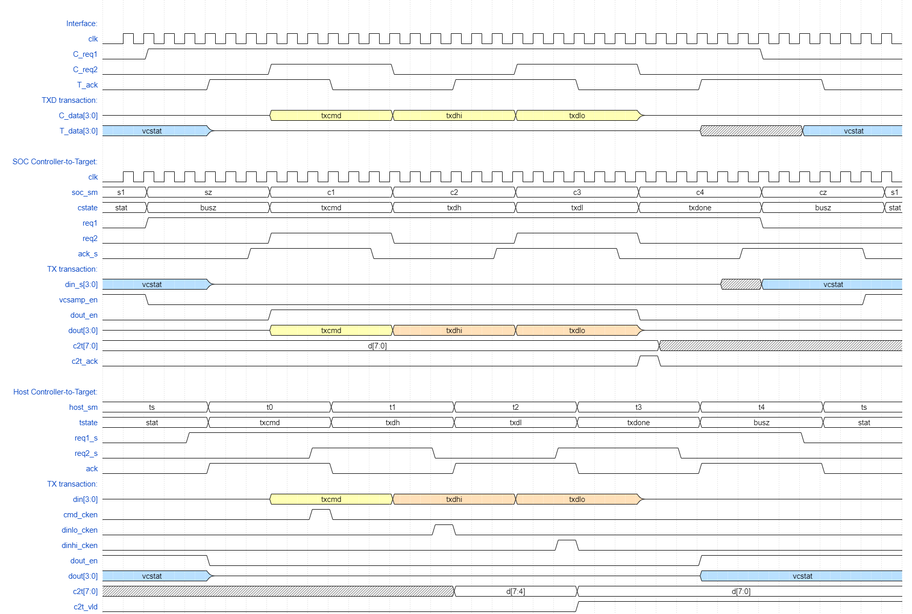
Hostio4 communication protocol waveforms
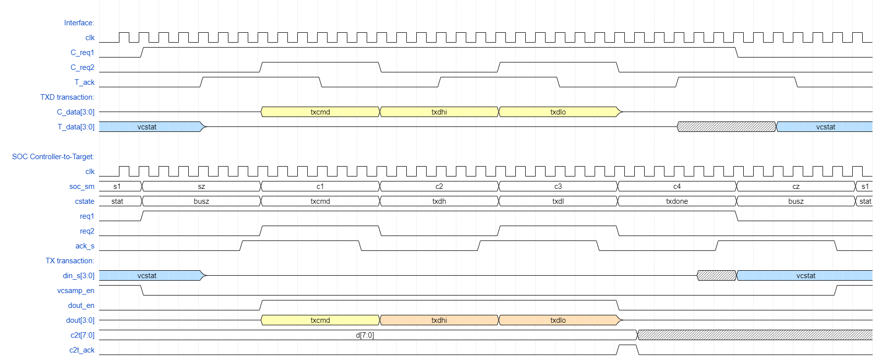
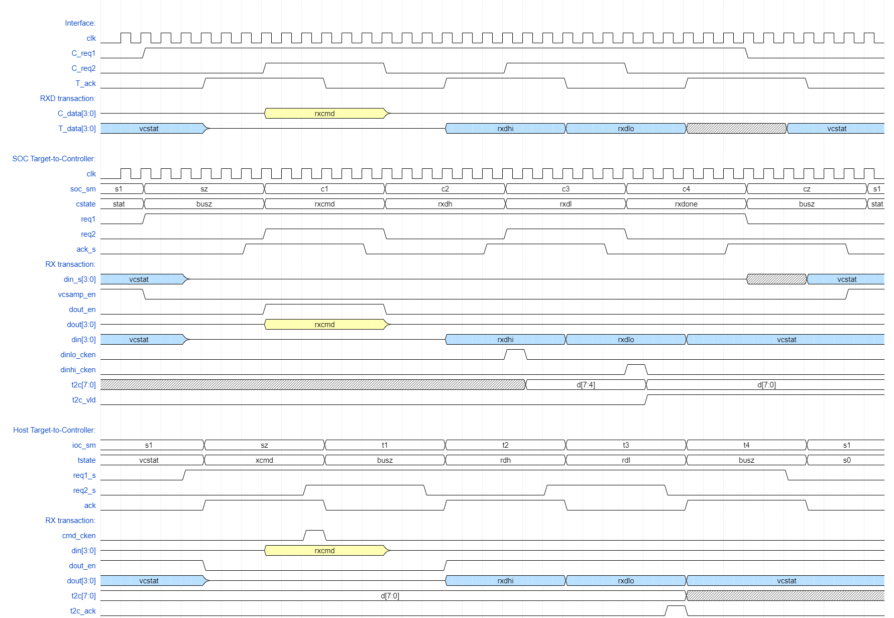
A packet protocol handles the transfer of status, commands and high- and low-nibbles of data with safe tristate-bus turnaround. The basic packet transfer protocol shown in the time domain is as follows:
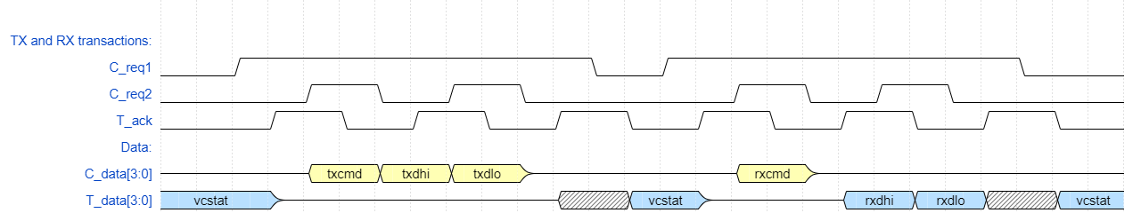
Each change of Request signalling transition results in the Acknowledge toggling (synchronized "_s" version seen at the SoC) only when the bidirectional data bus is enabled, sampled, or disabled as appropriate.
In the receive case the SoC initiates the transfer sequence when the host virtual channel receive ready status is valid and there is a byte of control or data to transfer to the host:
in the case when the host virtual channel transmit ready status is valid and there is room in the the appropriate channel receive stream buffer then the SoC transaction behaves as follows:
Hostio4 chiplet mode selection
Building on the basis of a global reset being distributed to multiple chips or chiplets, once all SoCs have been reset then all the REQ1/2 outputs are tri-stated as undriven and only the specific chiplet receives XACK driven low will become selected and enable the drive to the REQ1/REQ2 request signals.
At the test interface pull-down resistors would be be added to the multi-driver REQ1, REQ2 shared signals to hold the interface in a quiescent state from reset and each individual handshake ACK signal is linked to either VDDIO or the target state machine ACK output.
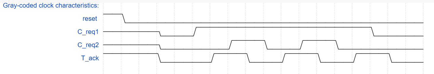
Clocking
The hostio interface assume asynchronous clocking for the SoC Initiator and the Host Target design, and the clocking strategy simply derives the acknowledge handshake behaviour based on the Gray-coded request signalling:
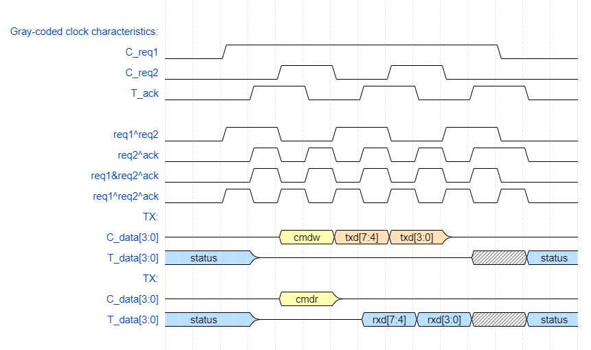
Implementation and validation details
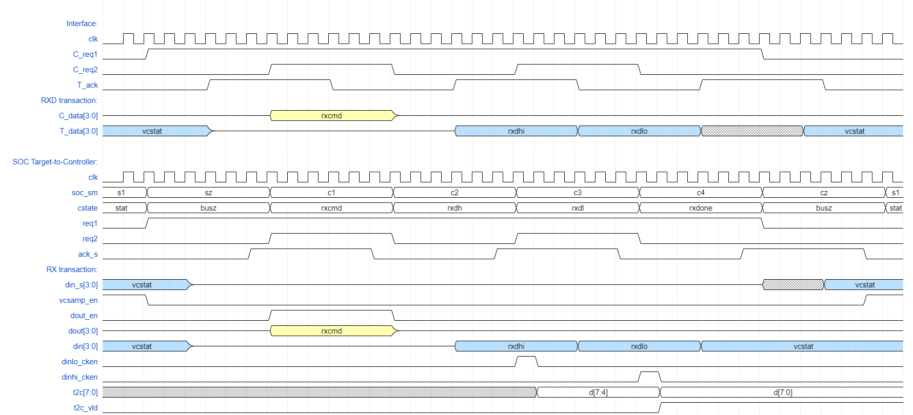
In detail the behaviour at the SoC Initiator and Host Target are shown in more detail for the RX and TX cases below:
IP github repository
The HOSTIO4 IP is independently packaged and maintained at: https://git.soton.ac.uk/soclabs/hostio4
Explore This Technology

Projects Using This Technology

Comments
Diagram titles added
Alternative text provided
Add new comment
To post a comment on this article, please log in to your account. New users can create an account.