TSRI Arm Cortex-M55 AIoT SoC Design Platform
What is TSRI Arm Cortex-M55 AIoT SoC Design Platform?
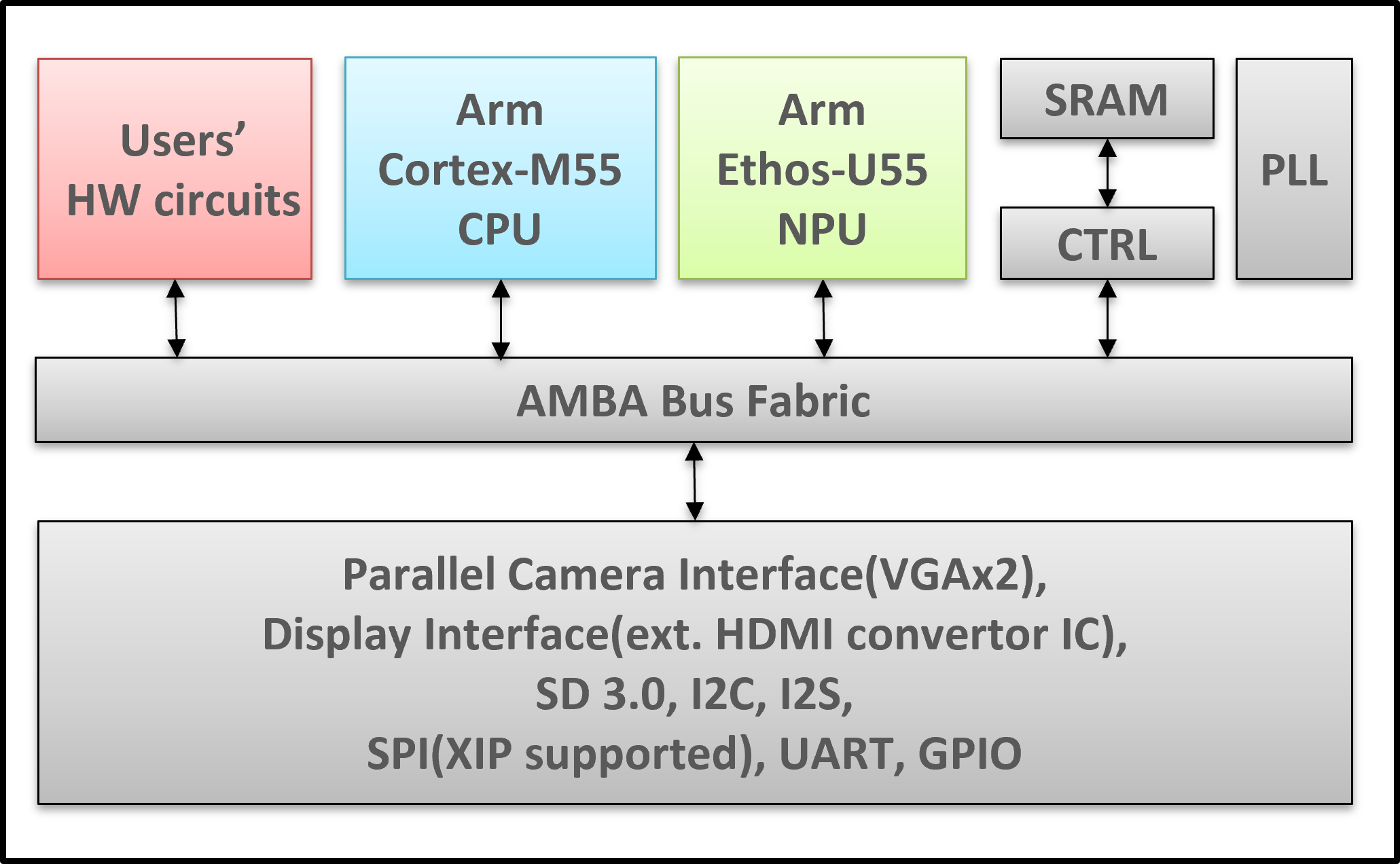
The Arm Cortex-M55 AIoT SoC design platform is an AIoT subsystem that allows custom SoC designers to integrate their hardware circuits and embedded software for differentiation. The platform is developed by TSRI (Taiwan Semiconductor Research Institute) to support academic research on SoC design. It's built on the Arm Corstone-300 reference package, featuring the Cortex-M55 CPU and Ethos-U55 NPU. The platform is equipped with popular peripherals such as camera input, video output, and audio in/out, enabling support for a wide range of applications.
Features Highlights
- Silicon proven - 16nm reference design
- System ready - EVB, bare-metal BSP, sample systems for AI applications (Yolo-fastest object detection and keyword spotting)
- FPGA prototyping system available
- Lower the technical barrier of custom SoC design
- Accelerate time to tape-out/publication
SoC Specification
| Arm Cortex-M55 CPU | I/D cache size: 32KB, I/D TCM size: 512KB |
| Arm Ethos-U55 NPU | MACs #: 256, Internal memory size: 512 KB |
| SRAM | On chip memory size: 2MB |
| User's HW Circuits | Interface: AMBA AXI3 (default: 64 bits data, 32 bits address) |
| Peripherals | As shown in Fig. 1 |
| Clock rate | 200MHz (w/o PLL) / 666MHz (w/ PLL) |
| External memory (Boot) | QSPI flash memory size: 8MB |
SoC Memory Map
The memory map follows the guide of "Memory map overview for Corstone™ SSE-300". (https://developer.arm.com/documentation/100966/1127/Arm--Corstone-SSE-300-FVP/Memory-map-overview-for-Corstone-SSE-300)
| Non-security Area | |||
| Address | Range | Description | |
| 0x0000_0000 | 0x8_0000 | ITCM | 512KB |
| 0x0100_0000 | 0x20_0000 | BRAM | 2MB common SRAM |
| 0x2000_0000 | 0x8_0000 | DTCM | 512KB (None Security) |
| 0x2100_0000 | 0x8_0000 | SRAM | 512KB SSE300 internal SRAM (U55) |
| 0x3000_0000 | 0x80_0000 | QSPI | 8MB quad spi flash |
| 0x4000_0000 | 0x1000 | GPIO | General purpose IO 0~15 |
| 0x4140_0000 | 0x1000 | Ethernet | Pseudo sram bus interface |
| 0x4141_0000 | 0x1000 | USB | Pseudo sram bus interface |
| 0x4180_0000 | 0x1000 | QSPI | QSPI Config AHB slave interface |
| 0x4190_0000 | 0x1000 | QSPI | QSPI Write AHB slave interface |
| 0x41a0_0000 | 0x1000 | SD | TSRI user SD2.0 controller interface |
| 0x41b0_0000 | 0x1000 | AIIP | AI IP controller AHB slave interface |
| 0x41c0_0000 | 0x1000 | HDLCD | TSRI color LCD AHB slave interface |
| 0x41d0_0000 | 0x1000 | OSD/PLL | Use unused register space 0x800 ~ 0x80B for PLL configuration |
| 0x4130_0000 | 0x1000 | SENSOR | TSRI sensor controller interface |
| 0x4131_0000 | 0x1000 | IMAGE | TSRI image controller interface |
| 0x4139_0000 | 0x2000 | LINE0 | TSRI image line buffer 0 space |
| 0x413a_0000 | 0x2000 | LINE1 | TSRI image line buffer 1 space |
| 0x413b_0000 | 0x1000 | DMA | TSRI AHB DMA controller interface (PL081) |
| 0x413c_0000 | 0x1000 | U55 | U55 APB slave interface |
| 0x4920_0000 | 0x1000 | I2C | Touch panel I2C interface |
| 0x4921_0000 | 0x1000 | I2C | Audio I2C interface |
| 0x4922_0000 | 0x1000 | I2C | Camera I2C interface |
| 0x4923_0000 | 0x1000 | I2C | HDMI I2C interface |
| 0x4924_0000 | 0x1000 | SCC | System configuration controller |
| 0x4925_0000 | 0x1000 | I2C | Audio I2S controller |
| 0x4930_0000 | 0x1000 | LED | User LED controller |
| 0x4931_0000 | 0x1000 | UART | uart 0 |
| 0x4932_0000 | 0x1000 | UART | uart 1 |
| 0x4933_0000 | 0x1000 | CLCD | TFT QVGA color LCD controller |
| 0x4934_0000 | 0x1000 | RTC | real time clock controller |
| 0xA000_0000 | 0x1000_0000 | HYPRAM | maximum 256MB TSRI hyper ram (64MBx4) |
| Security Area | |||
| Address | Range | Description | |
| 0x3000_0000 | 0x8_0000 | DTCM | 512KB |
| 0x3100_0000 | 0x8_0000 | SRAM | 512KB SSE300 internal SRAM (U55) |
| 0x3800_0000 | 0x80_0000 | QSPI | 8MB quad spi flash |
| 0x5110_0000 | 0x1000 | GPIO | General purpose IO 0~15 |
| 0x5140_0000 | 0x1000 | Ethernet | Pseudo sram bus interface |
| 0x5150_0000 | 0x1000 | USB | Pseudo sram bus interface |
| 0x5180_0000 | 0x1000 | QSPI | QSPI Config AHB slave interface |
| 0x5180_1000 | 0x1000 | QSPI | QSPI Write AHB slave interface |
| 0x5180_2000 | 0x1000 | SD | TSRI user SD2.0 controller interface |
| 0x5120_0000 | 0x1000 | AIIP | AI IP controller AHB slave interface |
| 0x5120_5000 | 0x1000 | HDLCD | TSRI color LCD AHB slave interface |
| 0x5120_6000 | 0x1000 | SENSOR | TSRI sensor controller interface |
| 0x5130_0000 | 0x2000 | IMAGE | TSRI image controller interface |
| 0x5130_2000 | 0x2000 | LINE0 | TSRI image line buffer 0 space |
| 0x5130_4000 | 0x2000 | LINE1 | TSRI image line buffer 1 space |
| 0x5140_0000 | 0x1000 | DMA | TSRI AHB DMA controller interface (PL081) |
| 0x5810_0000 | 0x1000 | U55 | U55 APB slave interface |
| 0x5920_0000 | 0x1000 | I2C | Touch panel I2C interface |
| 0x5921_0000 | 0x1000 | I2C | Audio I2C interface |
| 0x5925_0000 | 0x1000 | I2C | Camera I2C interface |
| 0x5926_0000 | 0x1000 | I2C | HDMI I2C interface |
| 0x5930_0000 | 0x1000 | SCC | System configuration controller |
| 0x5931_0000 | 0x1000 | I2S | Audio I2S controller |
| 0x5930_3000 | 0x1000 | LED | User LED controller |
| 0x5930_4000 | 0x1000 | UART | uart 0 |
| 0x5930_5000 | 0x1000 | UART | uart 1 |
| 0x5930_6000 | 0x1000 | CLCD | TFT QVGA color LCD controller |
| 0x5930_7000 | 0x1000 | RTC | real time clock controller |
| 0xB000_0000 | 0x1000_0000 | HYPRAM | maximum 256MB TSRI hyper ram (64MBx4) |
Users' HW circuits design, SoC integration and simulation
Users can design their own HW circuits to accelerate computing for specific application processing, such as object detection, generative AI, cryptography, and DNA sequencing data analysis. Users can replace the built-in Ethos-U55 NPU with thier own NPU if necessary. Their HW circuits must have an AMBA interface to be integrated into the TSRI Arm Cortex-M55 AIoT SoC design platform.
Users can easily integrate their own HW circuits into the TSRI Arm Cortex-M55 AIoT SoC design platform and start the whole SoC simulation by following these steps.
- Before integrating users' HW circuits, run out-of-box testing to ensure the environment for SoC integration and whole SoC simulation is installed properly.
- Replace the dummy RTL code with users' own RTL code of HW circuits. Make sure the RTL code is well verified by simulation before going to this step. It is highly recommended to use Verification IP for AMBA bus interface compliance checks.
- Develop the embedded SW/FW based on the given environment and sample code, which is part of TSRI Arm Cortex-M55 AIoT SoC design platform. Arm Development Studio will be used for SW/FW development.
- Change to working mode from test mode by undefine a parameter.
- Run simulation. Cadence Xcelium Logic Simulator or Synopsys VCS will be used for simulation. Synopsys Verdi will be used for debug.
FPGA Prototyping
It's almost impossible to fully verify the function of the whole SoC by simulation only due to the long simulation time. FPGA prototyping will be used to speed up verification and for early software bring-up as well. The FPGA prototyping system allows designers to implement and test their designs on reconfigurable FPGA hardware before committing to final silicon. TSRI use Arm MPS3 FPGA Prototyping Board for FPGA prototyping of Arm Cortex-M55 AIoT SoC design platform. A camera module and a display module were developed by TSRI and added to the Arm MPS3 FPGA Prototyping Board for real-time video application development.
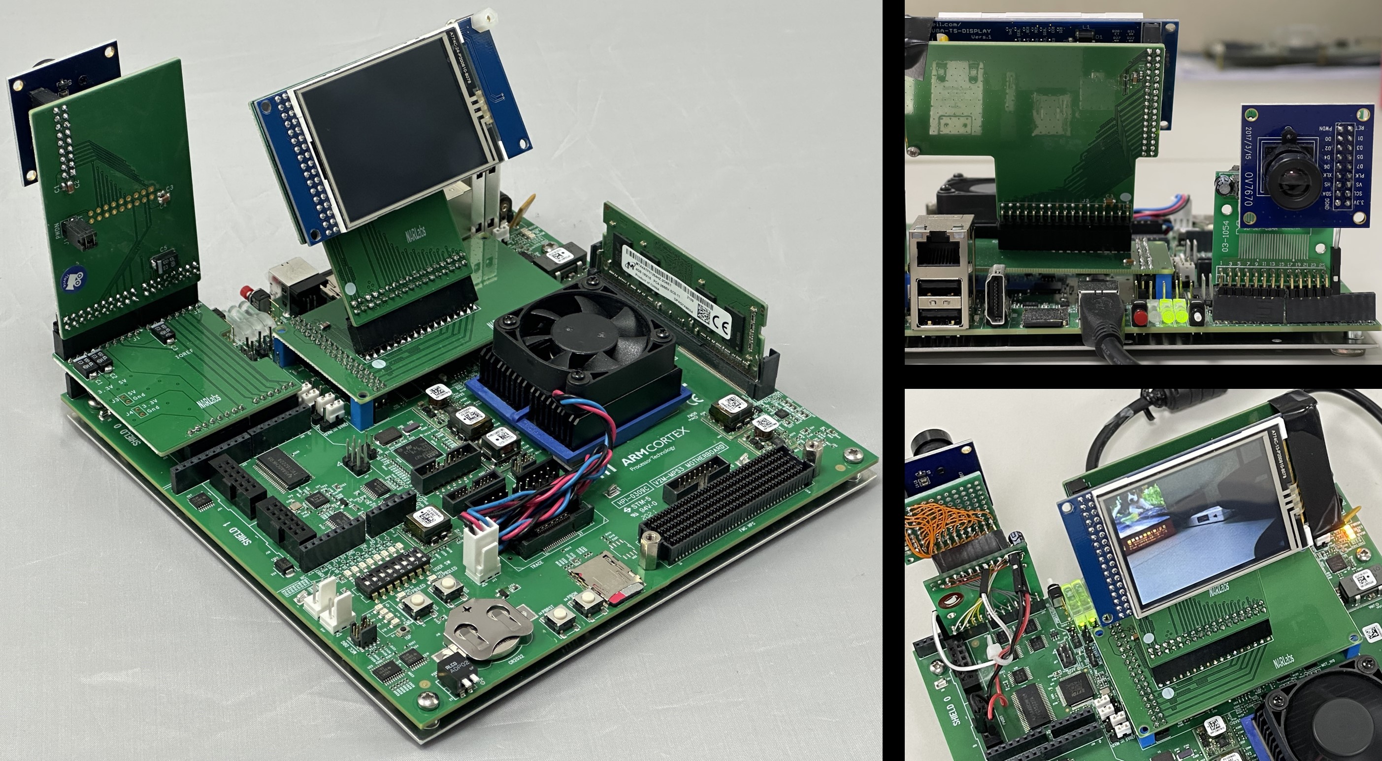
Fig. 1- FPGA Prototyping System
Synopsys Synplify Premier and Xilinx Vivado will be used for FPGA prototyping. The maximum clock rate of this FPGA prototyping system is 50MHz. The FPGA utlization is as follows.
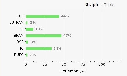
Fig. 2- FPGA Utilization of TSRI Arm Cortex-M55 AIoT SoC design platform
16nm Reference Design RTL to GDS(R2G) Implementation and Verification
A 16nm reference design was taped out for manufacturing. After the sign-off of RTL code of the whole SoC (that means RTL code is well verified either by simulation or FPGA prototyping), TSRI started R2G implementation and verification. Synopsys Design Compiler was used for the logic implementation (Logic Synthesis). Cadence Innovus was used for the physical implementation (APR/Automatic Placement & Routing). Synopsys PrimeTime was used for the static timing analysis (STA). The complete SoC design flow is illustrated as follows.
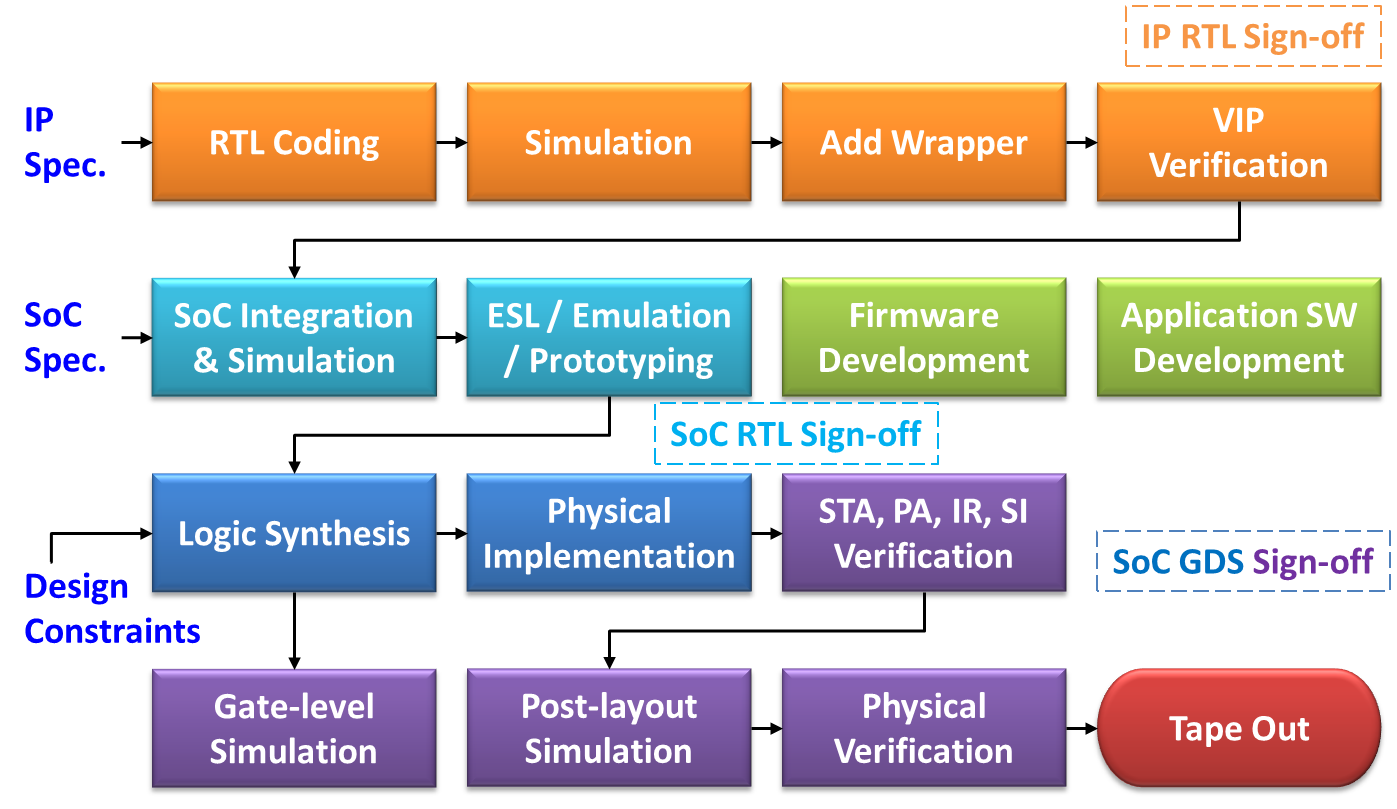
Fig. 3- SoC Design Flow
The layout of the taped out design is as shown below.
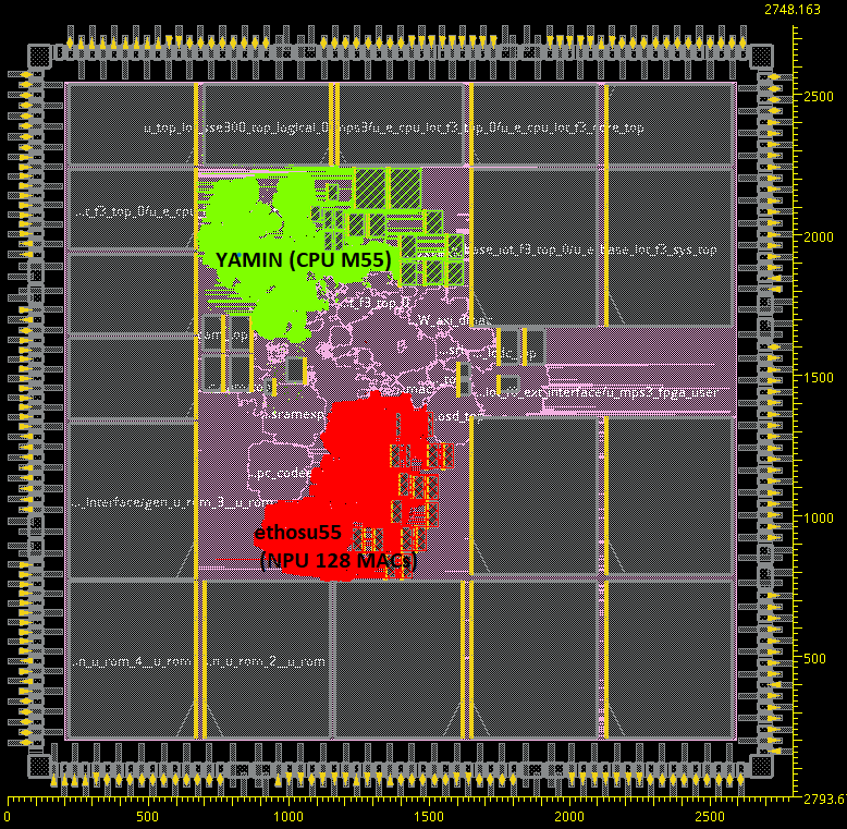
Fig. 4- SoC Layout
The statistics of the 16nm reference design implementation are as shown below.
| Process | TSMC 16nm FinFET Compact Technology (16FFC) |
| Metal Scheme | 11M, 2Xa1Xd3Xe2Y2R |
| Library Corners | 0.72v -40℃, 0.72v 125℃, 0.88v -40℃, 0.88v 125℃ |
| RC Corners | rcworst CCworst, cworst CCworst, rcbest CCbest, cbest CCbest |
| Chip Area | 2794um x 2747um |
| Instance # | Std. cells: 1M, SRAMS: 62 (4MB) CPU I/D TCM: 512KB/512KB, NPU: 256KBx2, Buffer: 2MB |
| IO Pad # | Signals: 221, Core P/G: 8, IO P/G:8 |
| Clock # | Intrinsic: 8, Generated: 13 |
| Max. Clock Freq. | 200MHz (rev. 666MHz w/ PLL) |
The runtime for the physical implementation is 44 hours in terms of real time and 326 hours in terms of CPU time. The multi-core option was turned on when running EDA tools, with the core (thread) number set to 64. The elapsed time for each stage is shown below.
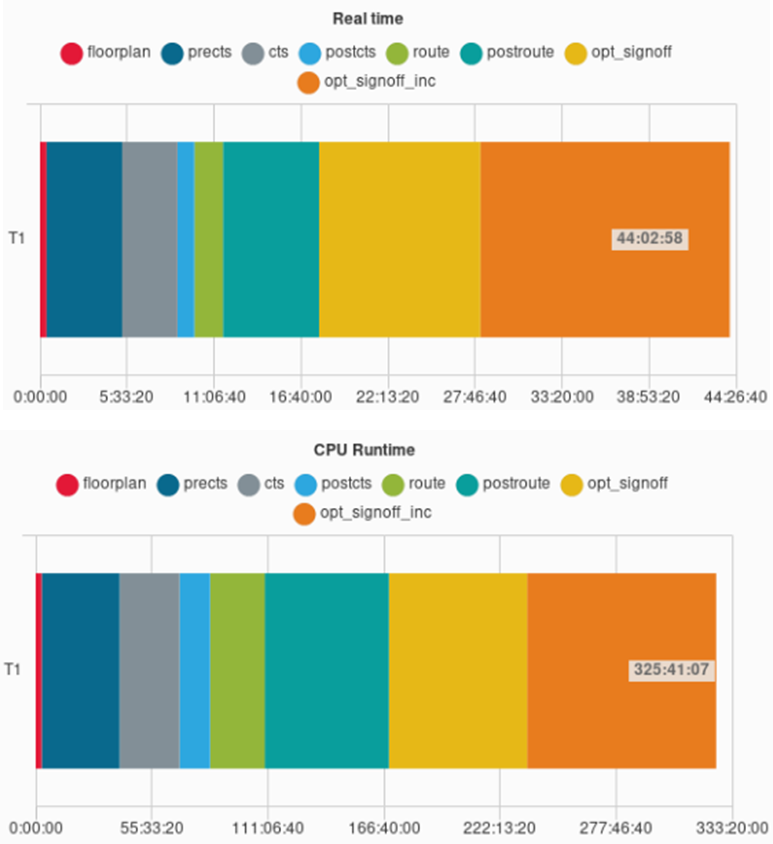
Fig. 5- Runtime of each stage of the physical implementation
ASIC and Evaluation Board(EVB)
The manufactured chip was tested on EVB TSRI developed. The validation system worked well. CPU, NPU and all periherals including video and audio in/out worked properly.
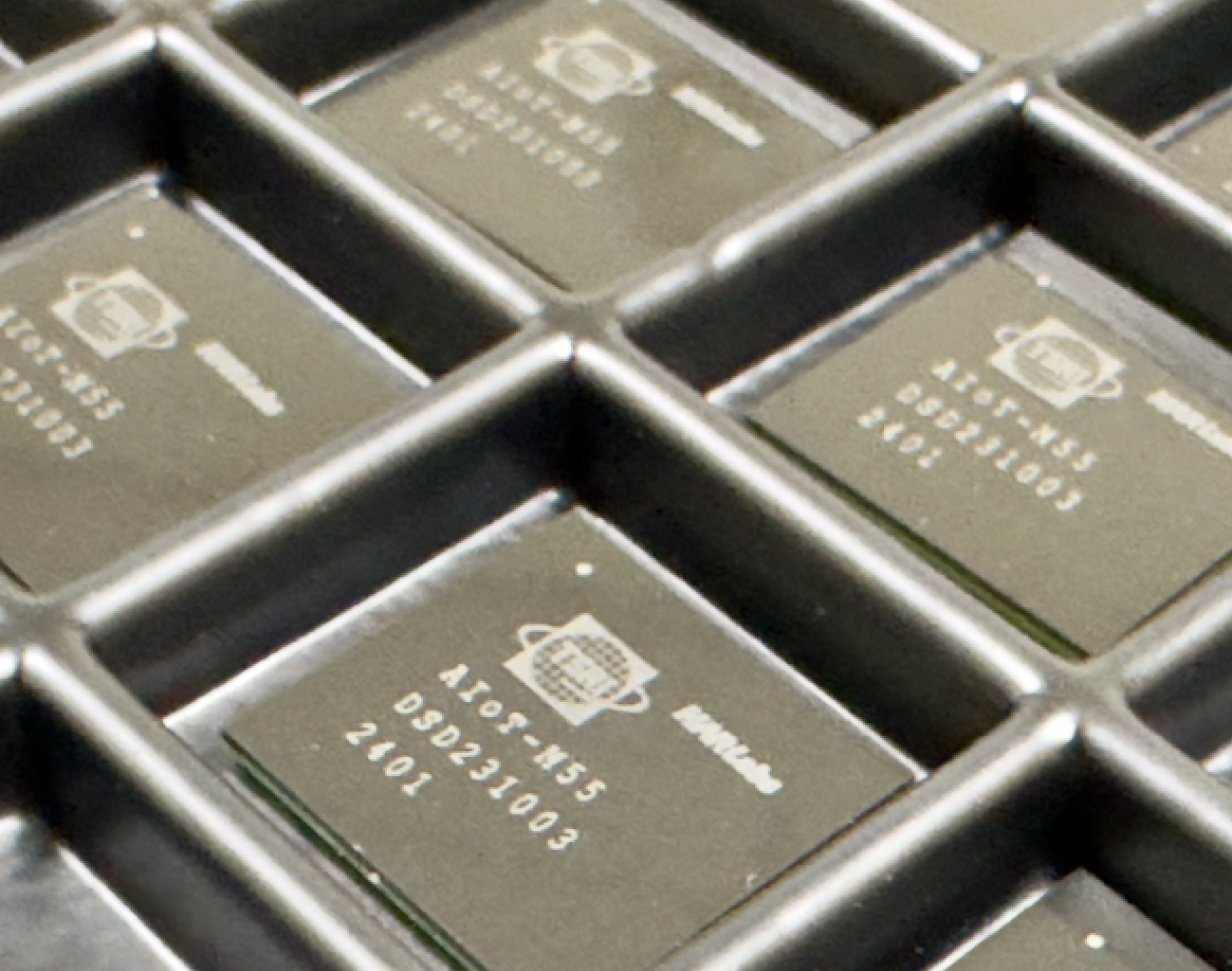
Fig. 6- The Silicon
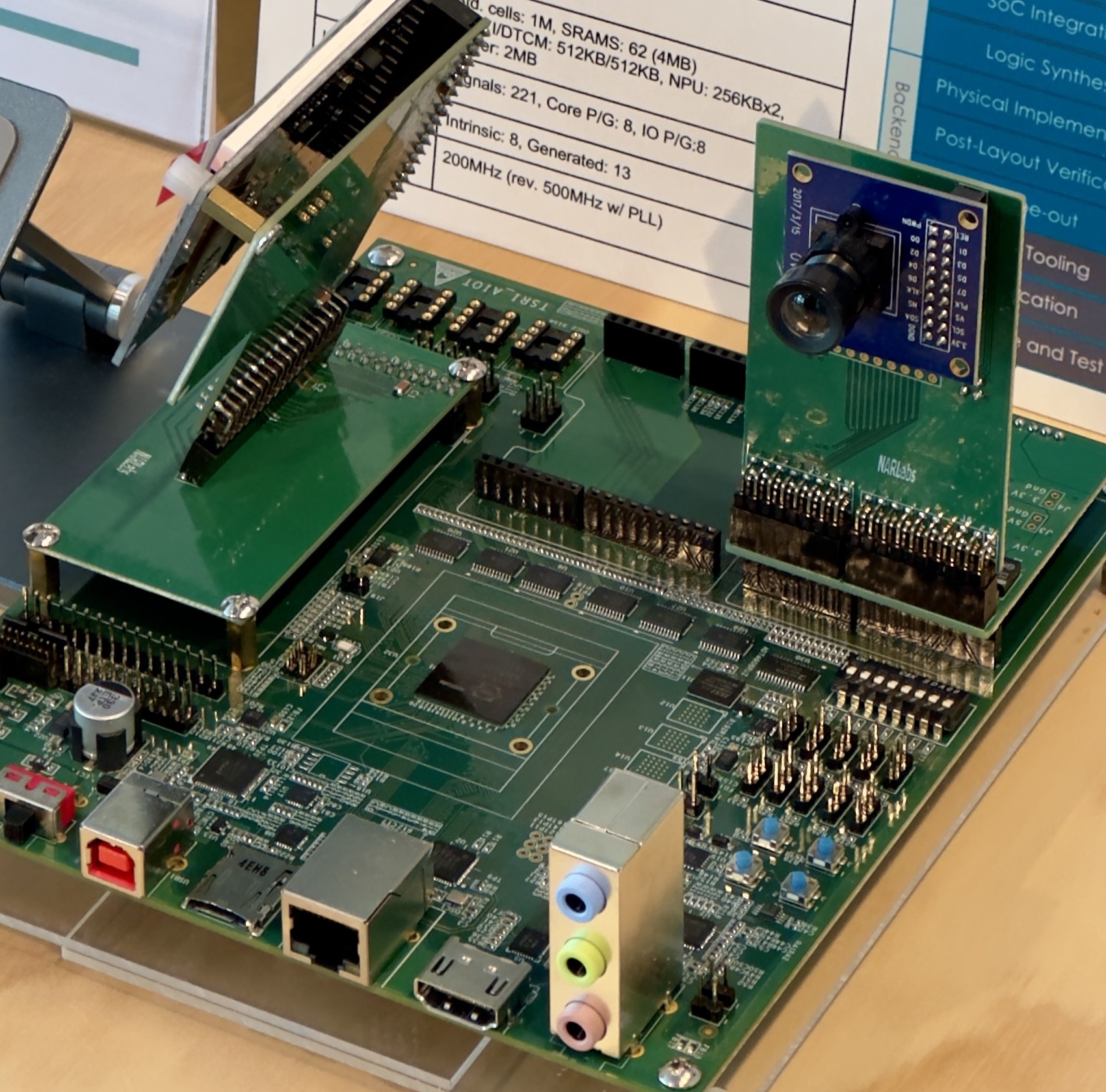
Fig. 7- The EVB
Sample Systems for AI applications
- Yolo-fastest object detection
- KWS (KeyWord Spotting)
Using TSRI Arm Cortex-M55 AIoT SoC Design Platform
Taiwan's research teams are all eligible to use the TSRI Arm Cortex-M55 AIoT SoC Design Platform. Overseas research teams may access the TSRI SoC design platform through collaborations with Taiwan's research teams. This is upon request and requires TSRI's approval. Since the platform contains Arm IP, the professor leading the research team must be an AAA (Arm Academic Access) member. Membership is free of charge. Refer to the following link for details of the AAA program.
https://www.arm.com/en/resources/research/enablement/academic-access
The TSRI Arm Cortex-M55 AIoT SoC Design Platform can only be used in the TSRI cloud. Users' data cannot be downloaded to protect the valuable silicon IP accessible in the cloud. The overview of TSRI's cloud is shown below.
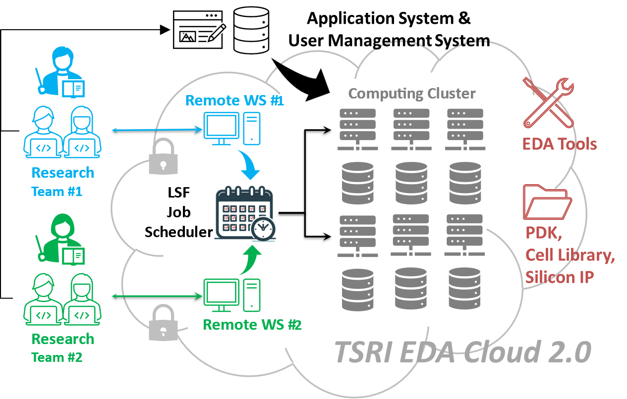
Fig. 8- TSRI's EDA Cloud for SoC design
Future Work
The silicon we currently have does not include a PLL. We have integrated the PLL into the TSRI Arm Cortex-M55 AIoT SoC design platform and have been working on a new reference design, which will be taped out in 2025. Universities' HW circuits may be integrated into the new reference design. The options of the target 16nm technology will be slightly modified to comply with the TSMC University FinFET program offering. Refer to the following link for details of the TSMC University FinFET program.
https://www.tsmc.com/english/dedicatedFoundry/services/university_program
After that, TSRI will collaborate with partners from industry and academia to develop SoC design training courses based on the new reference design.
Add new comment
To post a comment on this article, please log in to your account. New users can create an account.