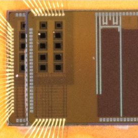
COILS-C1 65nm SoC with M0 cores in 3D stack
Low-cost 3D die stacking using near-field wireless communication.
This two-tier SoC, fabricated using a TSMC 65nm process, incorporates two Arm Cortex M0 CPU cores in addition to a wireless vertical AHB lite bus for inter-layer power and data transfer. The wireless AHB-Lite bus consists of four, 250um diameter, inductive channels to simultaneously transmit data (at speeds up to 6Gbps) and wirelessly transfer power, whilst also allowing ‘plug-and-play’ integration with existing SoC AHB-Lite peripherals.
The ability to deliver power and data wirelessly between layers of a 3D stack enables several dies (each of which may be fabricated in different process technologies) to be interconnected without including expensive, foundry-specific die-to-die interface technologies such as Through Silicon Vias (TSVs). Instead, dies can be simply picked and stacked using adhesive with significantly relaxed tolerances (and hence much lower cost).
To achieve concurrent Data and Power (DAP) transmission through a single Inductive Coupling Link (ICL), the proposed COILS-C1 design uses a Bi-Phase Shift Keying (BPSK) modulator to encode data in terms of phase, whilst recovering power from the high-frequency carrier signal. The links communicate across a total distance of 80um (70um die thickness + 10um glue thickness) and achieve 20.3Gbps/mm2 of data and 7.1mW/mm2 of power transfer. The chip also contains an on-board wireless clock interface to keep each die in the 3D stack precisely synchronised.
Using this approach, test-chip measurements show a 7.8x reduction in area compared with prior art (making this the smallest ever reported inductive power and data link). This work also represents the first instance of inductive links being integrated using a standard SoC bus protocol.


 Cortex-M0
 Peripherals
Add new comment
To post a comment on this article, please log in to your account. New users can create an account.