Building system-optimised AMBA interconnect
Bus fundamentals
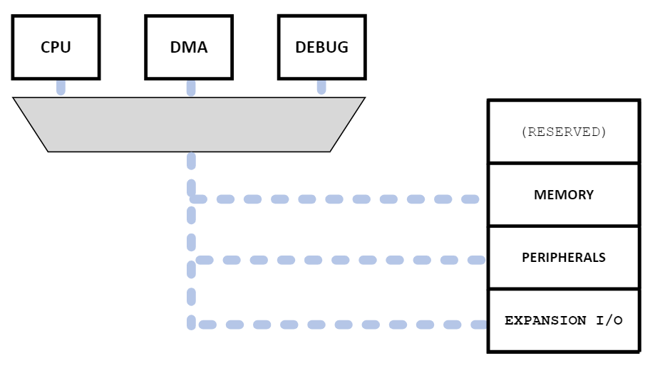
Basic bus-oriented systems start with the premise that a bus transaction Initiator (called 'Master' in the Arm tools and documentation) addresses one of a number of memory-mapped Target responders (traditionally called 'Slaves' in the Arm tools and documentation). With the addition of one or more other Initiators an arbitration mechanism has to be introduced which ensures some form of priority scheme is provided that allows different initiators to share the 'bus' fabric according to system-specific requirements.
The address width of the system depends on the largest addressing range of the initiators (typically 32-bit for Cortex M-class; the data transfer width is typically 32- or 64-bit, or maybe 128- or 256-but wide for computational accelerators.
Typically the bandwidth and access latency (or latencies) of the bus system must be carefully planned to understand real-time performance and bottlenecks, and in cases where a simple un-cached microprocessor requires much of the system bandwidth for code fetching the impact on interrupt service software routines has to be analysed carefully.
Multi-layer interconnect
An alternative approach is to provide multiple parallel interconnect "layers" such that independent Initiators can communicate concurrently with the particular memory-mapped target peripherals or subsystems. For example if the control microprocessor has an independent pathway to access Read-Only Memory (ROM) much of the code-fetch bandwidth is handled on the code 'layer' of the interconnect while a Direct Memory Access (DMA) device can have non-conflicting access to DMA memory buffers and peripherals.
System Random Access read/write Memory (RAM) is then shared by a number of layers of interconnect, so the arbitration is effectively at the addressed Target region. Where the system RAM is heavily used by both processor and acceleration or display subsystems then multiple sub-banks - or interleaved RAM banks can be a useful technique for minimising contention for shared target resources.
Multi-Layer AHB matrix generation
The AAA portfolio Arm provides scripts to generate system-optimised Bus Matrix components from XML textual specifications. A recommended starting point is in the Corstone-101 'bundle':
When unpacked the "BP210" Cortex-M System Design Kit (CMSDK) sub-bundle contains the IP, scripts and example XML:
Corstone-101_Foundation_IP/BP210-BU-00000-r1p1-00rel0/logical/cmsdk_ahb_busmatrix/
Arm documentation is provided in the main CMSDK Technical Reference Manual:
Corstone-101_Foundation_IP/BP210-BU-00000-r1p1-00rel0/documentation/Cortex-MSystemDesignKit_TechnicalReferenceManual_DDI0479D_r1p1-00rel0.pd
Case-study
soclabs 'nanosoc' interconnect
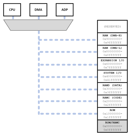
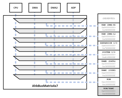
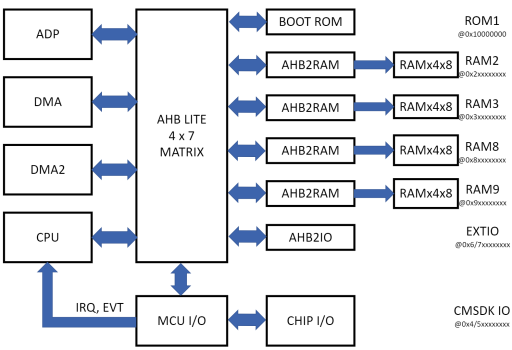
The example described here provides a bus-matrix developed for a system with four primary initiators:
- Cortex-M0 CPU
- ASCII Debug Protocol hardware debugger
- 2 x Direct Memory Access controllers
And seven distinct memory-mapped target subsystems:
- Boot ROM
- Code RAM
- Data RAM
- System IO peripherals
- DMA memory buffer 1
- DMA memory buffer 2
- Expansion (Accelerator) IO mapped hardware
The Boot ROM is required by the CPU at power-up reset but is also made visible to the ADP hardware system debugger to facilitate chip bring-up and testing. (Conventionally mapped at address 0 of the 32-bit address map)
The Code RAM supports uploaded test programs and diagnostics run on the CPU and typically needs to be mapped over the bootstrap ROM (to allow reprogramming of the software and interrupt servicing vectors) but is not needed by the DMA controllers.
The DMA memory buffers are primarily provided for zero-latency direct memory access traffic into and out-of the accelerator hardware that the chip supports, but does also require the CPU (and ADP) controllers to have access to setup, inspect and verify buffer transfers, but normal mode of operation are managed in software to avoid conflicting accesses during real-time operation.
xml file specification
Arm provides example xml files in the IP directory and descriptions of the specification directives in the Technical Reference Manual.
This section documents how the
A set of global declarations set up the interconnect generation specifications and file naming definitions (to allow multiple interconnect implementations to have name-space uniqueness).
<cfgfile>
<!-- Global definitions -->
<architecture_version>ahb2</architecture_version>
<arbitration_scheme>burst</arbitration_scheme>
<routing_data_width>32</routing_data_width>
<routing_address_width>32</routing_address_width>
<user_signal_width>2</user_signal_width>
<bus_matrix_name>soclabs_4x7_AhbMatrix</bus_matrix_name>
<input_stage_name>soclabs_4x7_MasterInput</input_stage_name>
<matrix_decode_name>soclabs_4x7_MatrixDecode</matrix_decode_name>
<output_arbiter_name>soclabs_4x7_Arbiter</output_arbiter_name>
<output_stage_name>soclabs_4x7_SlaveOutput</output_stage_name>
Then the target addressable/accessible regions are defined - in this case shown for the CPU microprocessor:
<!-- Slave interface definitions -->
<slave_interface name="_cpu">
<sparse_connect interface="_rom1"/>
<sparse_connect interface="_ram2"/>
<sparse_connect interface="_ram3"/>
<sparse_connect interface="_sys"/>
<sparse_connect interface="_exp"/>
<sparse_connect interface="_ram8"/>
<sparse_connect interface="_ram9"/>
followed by the system-specific memory map decoding regions:
<address_region interface="_rom1" mem_lo='00000000' mem_hi='0fffffff' remapping='move'/>
<address_region interface="_rom1" mem_lo='10000000' mem_hi='1fffffff' remapping='none'/>
<address_region interface="_ram2" mem_lo='20000000' mem_hi='2fffffff' remapping='none'/>
<address_region interface="_ram3" mem_lo='30000000' mem_hi='3fffffff' remapping='none'/>
<address_region interface="_sys" mem_lo='40000000' mem_hi='5fffffff' remapping='none'/>
<address_region interface="_exp" mem_lo='60000000' mem_hi='7fffffff' remapping='none'/>
<address_region interface="_ram8" mem_lo='80000000' mem_hi='8fffffff' remapping='none'/>
<address_region interface="_ram9" mem_lo='90000000' mem_hi='9fffffff' remapping='none'/>
<address_region interface="_exp" mem_lo='a0000000' mem_hi='dfffffff' remapping='none'/>
<address_region interface="_sys" mem_lo='f0000000' mem_hi='f003ffff' remapping='none'/>
<remap_region interface="_ram2" mem_lo='00000000' mem_hi='0fffffff' bit='0'/>
</slave_interface>
In this case a "remap" parameter (bit-0) has been introduced to allow the RAM (decoded at 256 Mbyte region 0x2... to be remapped to location 0 overlaying the initial ROM1 boot memory alias.
Similar specifications for each Initiator for the set of matrix access paths must be provided. In the case of a DMA controller the example uses:
<slave_interface name="_dma2">
<sparse_connect interface="_rom1"/>
<sparse_connect interface="_ram2"/>
<sparse_connect interface="_ram3"/>
<sparse_connect interface="_sys"/>
<sparse_connect interface="_exp"/>
<sparse_connect interface="_ram8"/>
<sparse_connect interface="_ram9"/>
<address_region interface="_ram2" mem_lo='00000000' mem_hi='0fffffff' remapping='none'/>
<address_region interface="_rom1" mem_lo='10000000' mem_hi='1fffffff' remapping='none'/>
<address_region interface="_ram2" mem_lo='20000000' mem_hi='2fffffff' remapping='none'/>
<address_region interface="_ram3" mem_lo='30000000' mem_hi='3fffffff' remapping='none'/>
<address_region interface="_sys" mem_lo='40000000' mem_hi='5fffffff' remapping='none'/>
<address_region interface="_exp" mem_lo='60000000' mem_hi='7fffffff' remapping='none'/>
<address_region interface="_ram8" mem_lo='80000000' mem_hi='8fffffff' remapping='none'/>
<address_region interface="_ram9" mem_lo='90000000' mem_hi='9fffffff' remapping='none'/>
<address_region interface="_exp" mem_lo='a0000000' mem_hi='dfffffff' remapping='none'/>
</slave_interface>
At the completing of the file the Initiator access ports are defined:
<!-- Master interface definitions -->
<master_interface name="_rom1"/>
<master_interface name="_ram2"/>
<master_interface name="_ram3"/>
<master_interface name="_sys"/>
<master_interface name="_ram8"/>
<master_interface name="_ram9"/>
<master_interface name="_exp"/><!-- - - - - *** DO NOT MODIFY BELOW THIS LINE *** - - - - - - - - - - - -->
</cfgfile>
Running the generation script
The Arm Technical Reference Manual documents the tool usage, and a README.txt file is provided in the IP directory that details the (perl) script usage and file directory structure.
It is recommended that timescale directives are supressed and the example command-line usage shows IPXACT model generation as well as the synthesizable verilog RTL - as well as example of capturing the tool transcript into a log file:
bin/BuildBusMatrix.pl -notimescales -xmldir xml -cfg soclabs_ahb32_4x7.xml \
-ipxact -ipxactsrcdir=ipxact/src -ipxacttgtdir=ipxact/built \
-over -verbose >& soclabs_ahb32_4x7.log
 David Flynn
Consultant
at University of Southampton
Research area: Low power system design
 Cortex-M Series
![]() Hardware design
Hardware design
![]() Simulation
Simulation
![]() Synthesis
Synthesis
Submitted on
Add new comment
To post a comment on this article, please log in to your account. New users can create an account.