Characterization of a SPAD: Integrated with Mixed Quenching Circuit
CMOS image sensors (CIS) play a crucial role in the imaging industry. CIS produces low-quality images in low-light conditions. Single Photon Avalanche Diode (SPAD) is a device used for low-light imaging because of its ability to detect single photons of light. To detect a single light photon, SPAD is biased above its breakdown voltage (Gieger mode). When the photon hits the active area during Geiger mode, a significant reverse current (avalanche current) is observed. Upon detection of the photon, the SPAD must be quenched (by quenching circuits) below its breakdown voltage to prevent afterpulsing (false detection). For the next detection, the SPAD's bias voltage will again be raised above the breakdown voltage using the same quenching circuitry. SPAD-based sensors have a wide range of applications, including fluorescence microscopy, LIDAR, and quantum cryptography.
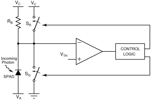
SPAD and Quenching Circuit:
SPAD breakdown voltage depends on their shape (circular, rectangular, octagonal) and types (P+/N-well, N-well/P-sub, P-well/Deep N-well). A SPAD structure incorporates guard rings to prevent premature edge breakdown. A mixed passive-active quenching circuit provides faster quenching (with transistors). Mixed quenching circuits reduce the afterpulsing phenomenon effectively. The integration of SPAD with a mixed quenching circuit improves performance (by reducing parasitics). SPAD performance can be a measure of photon detection efficiency (number of detected photons out of total incoming photons) or afterpulsing probability or timing resolution (how accurately SPAD measures incoming photon arrival time).
A mixed quenching circuit (fig. 1) connects SPAD to a ballast resistor (RB) and active quenching and reset circuit. When an avalanche is triggered, the avalanche current flows through the RB to quench the avalanche, similar to a passive quenching circuit. The active circuitry soon detects the avalanche and begins active quenching (by switching on the SQ switch). An SR switch resets the SPAD to its bias voltage.
Objective:
-
To design the different shapes and types of SPAD in a given technology node (65 nm).
-
To integrate the designed SPAD with a mixed quenching circuit and characterize SPAD structures based on photon detection efficiency, after pulsing probability, and timing resolution.
Team


 Project Creator
at International Institute of Information Technology, Hyderabad (IIITH)
Submitted on
Add new comment
To post a comment on this article, please log in to your account. New users can create an account.