milliSoC
milliSoc is ideal for a small academic team that want to evaluate research hardware in a SoC that can provide real-time processing for applications such as RF / radar signal processing, constrained AI models, low resolution real-time video processing. milliSoC is still under development and we welcome collaborations.
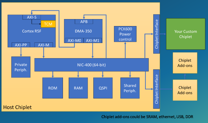
milliSoC is a mid-ranged reference design within SoC Labs. It provides a real-time system on Chip (SoC) using the Arm Cortex R5, that can be extended for design and evaluation of research blocks or subsystems. milliSoC is being designed as a reusable SoC design that can add memory-mapped experimental hardware, and follows the SoC Labs principle of simplifying the SoC design process with seamless transition from FPGA prototyping to physical silicon fabrication and evaluation.
For the software system, milliSoC is expected to utilise a real-time operating system, as opposed to the bare metal of nanoSoC or the linux operating system used for more complex A class SoC designs.
Reference Design Comparison Table
This table will let you compare this reference design with others on SoC Labs| Title | nanoSoC | milliSoC | megaSoC |
|---|---|---|---|
| Class | Entry | Mid Range | High End |
| Reference Design | nanoSoC | milliSoC | megaSoC/Corstone 1000 |
| Staffing | Single student / academic | Academic + dedicated post-doc | Academic Team |
| Time Scales | 6 months to 1 year | 1+ years | 18 Months - 3 Years |
| Model Forms | small | Real Time | Full Video/Large AI Model |
| Tape Out / Package and Board Costs | From 10k Euro | 25k-50k EUR | >50K - >>50K |
| Processor(s) | M0 | R5 | A53 |
| Processor(s) (speed) | <250 Mhz | 250-800 MHz | 1 GHz |
| Data Rates / On Chip Comms | <2.5 Gbps | 10-80 Gbps | >100 Gbps |
| Data Rates / Off Chip Comms | <50 Mbps | 0.1 - 0.8 Gbps | >1 Gbps |
| On Chip Memory Requirements | 32KB to sub MB | 2 MB+ | 4 MB+ |
| Virtual Prototype Environment | Xilinx ZCU104 | Arm MPS3 | HAPS |
| Tape Out Node | 65nm | 28nm | 16nm |
Related Projects and Workflows
This section details the following: the core reference design, the initial project that led to the definition of the reference design, and any additional projects that extend the reference design for new or additional applications. It also defines the related example workflows for the front end Architectural and Behavioural design stages, and the back end Logical and Physical design stages. Front end Behavioural design are usually accomplished with FPGA environments and tool chains, back end Physical design requires technology specific design rules and EDA tool suites.
Add new comment
To post a comment on this article, please log in to your account. New users can create an account.