nanoSoC
nanoSoC is the entry level reference design within SoC Labs. It is ideal for small academic projects that can be undertaken by PhD or other students to evaluate research hardware such as a custom accelerators or signal processing subsystems with a low cost of fabrication and evaluation. nanoSoC is silicon proven using the TSMC 65nm process.
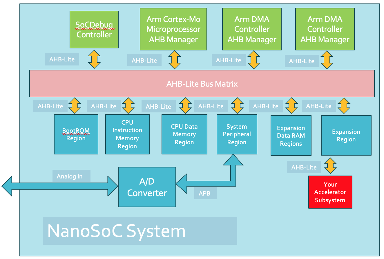
The core system for nanoSoC is a simple Arm Cortex M0 microcontroller System on Chip ("SoC") that can be easily extended for design and evaluation of research blocks or subsystems. nanoSoC has been architected to be a reusable SoC design that can add memory-mapped experimental hardware while simplifying the SoC design process with seamless transition from FPGA prototyping to physical silicon fabrication and evaluation using common verification methods throughout the design process. Our aim with nanoSoC is to provide a simple reusable design an entry point for academic projects that is easily adopted but covers all the grounding concepts in System on Chip design.
Version 1: The initial version of nanoSoC was architected for adding small custom acceleration hardware for Artificial Intelligence / Machin Learning applications as a base reference design for the SoC Design Contest for 2023 . It had optional DMA controllers to manage the movement of data on/off the custom accelerator. It had a simple power management architecture to allow measurement of energy consumption by the custom accelerator. It was extended to add a analog subsystem for the SoC Design Contest 2024/25.
Version 2: The second version of nanoSoC has added improvements in Host Communications ("HOSTIO") interconnect and improved power domain design which will allow better research measurements to be obtained.
Version 3: The third version of nanoSoC is being planned to expand the number and variety of subsystems, improve the ability to undertake Architectural/Behavioural Design exploration, ease uptake reducing the learning curve for people by simplifying design flow steps and refactoring the code repository.
How does nanoSoC extend the base Arm IP
A requirement in undertaking the design flow to specify nanoSoC was to simplify the transition from high level design prototyping using FPGAs to physical design and tape out for fabrication of real devices.
Modern industrial design practice has progressed beyond a stepwise refinement method to include more agile iterations and prototyping in high level design flows as well as the adoption of reusable design patterns. A key to support such method is always having at any stage a view of the design that can be verified and tested, often via Continuous Integration and Deployment for Verification. Such an approach requires not just starting the design process looking at major functional needs but starting with creating the basis of a deployable design as a starting point. Functional features can be added at any point knowing they can be deployed, verified and if necessary debugged.
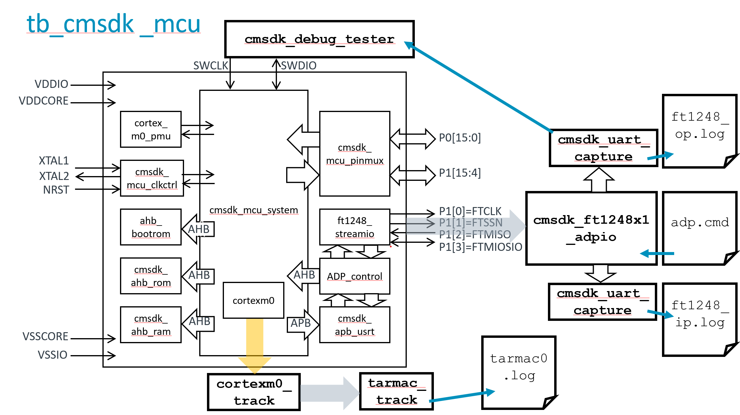
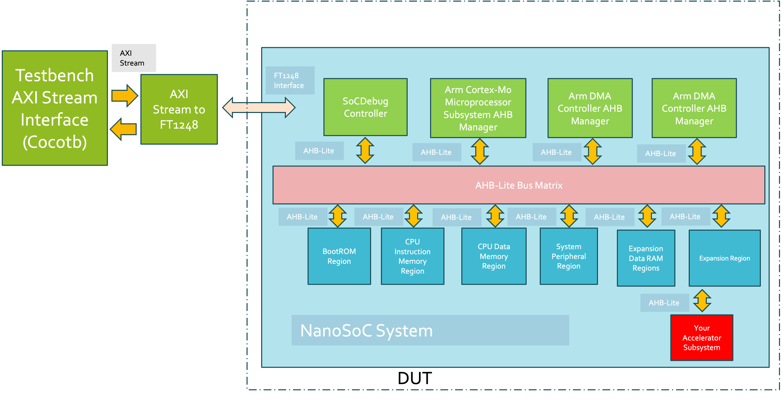
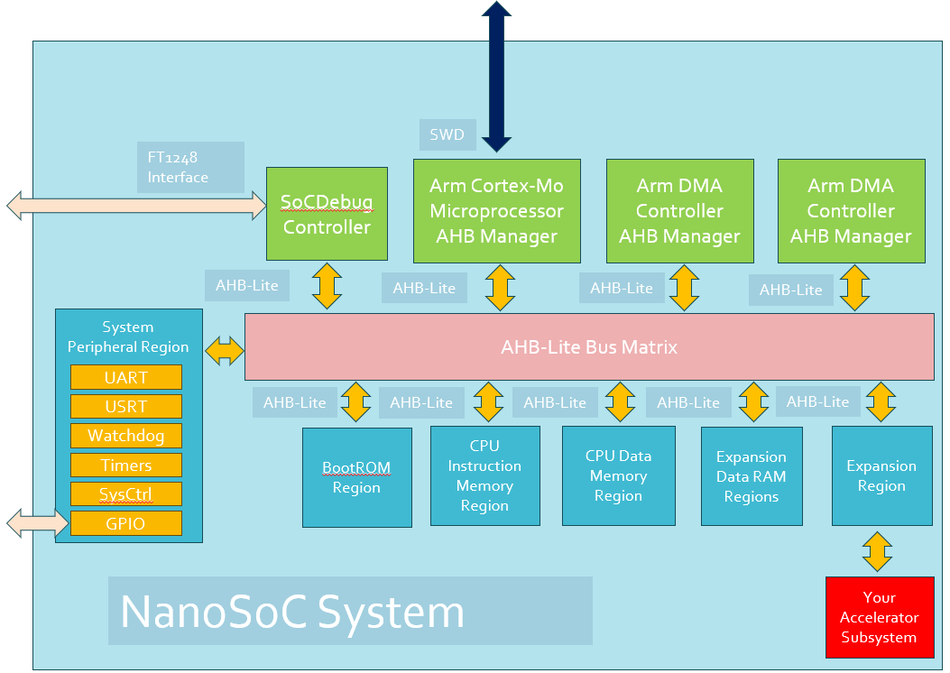
In the design flow to select ip for nanoSoC the cost both in fabrication and in human time and effort to design a SoC are important requirements. nanoSoC extends the Arm Cortex-M System Design Kit, CMSDK, which provides pre-verified IP blocks, associated software, verification assets and documentation. One modification is the addition to the arm Cortex-M0 microcontroller system of pad-ring support ready for silicon implementation. This supports ASIC evaluation and debug from early stages of the design process. The nanoSoC defines address map and bus matrix support expansion memory regions for experimental sub-systems. It also provides an FT1248 interface for off chip communication for external test bench supporting both FPGA and final ASIC hardware verification using common assets. A modified boot monitor and run-time software load process as well as "Tarmac" support for both RTL and gate-level tracing and external debug control allow verification throughout the design process.
By adopting the nanoSoC reference design an academic project can progress easily through the design process in an agile manner knowing that, if at a later stage a redesign of some aspect is necessary, the re-verification of the design is easily actioned. Throughout the design process, block-level designs and verification works in parallel with system and chip-level design and verification.
nanoSoC provides a reusable, deployable, verifiable, base reference design.
To access the nanosoc reference design you can use a 'git' installation for your own local project and download/clone the nanoSoC repository to your project using the command:
- git clone --recurse-submodules https://git.soton.ac.uk/soclabs/accelerator-project.git
PGA Flow for initial design stages
An aim of SoC Labs is to simplify transition from FPGA to full ASIC flow. While FPGA environments speed up initial design flow stages an over reliance on components within the Processing System fabric of the FPGA can act as a later barrier to full ASIC flow. The nanoSoC reference design and example FPGA design flow, instantiate a chip level just inside the pad-ring within the FPGA overlay that is independent of Xilinx system IP apart from basic provision of clocking and reset control. An AXI based "socket“ mimics pad ring connections to ensure the full SoC design is synthesizable, can be verified and is functional for an ASIC tape out.
Extending the nanoSoC reference design
There are a growing number of SoC Labs projects (see below) that extend the core nanoSoC reference design. The initial collection of projects using the nanoSoC design were implementing custom accelerators for Machine Learning based inference. Such IP extensions require very efficient transfer of data across the System of Chip bus fabric. The nanoSoC design can be extended by DMA controllers, such as the DMA 230, DMA 350 from Arm or custom controller IP. More recent project have been developing analog parts for subsystems such as sensing. Additional IP such as Analog to Digital Converters ("ADC") and Phase Locked Loops ("PLL") have been used to extend nanoSoC based system capabilities.
ASIC Flow for back end design stages
The nanoSoC reference design has been certified using a number of Electronic Design Automation suites from the major industry vendors as well as open source alternatives.
Verification
Students and academics can benefit from shared resources especially verification efforts which are often a weak point in academic projects. nanoSoC is based on the Arm Cortex-M System Design Kit (CMSDK) reference design which provides pre-verified IP and verification assets which can be extended. nanoSoC extends these to provide a continuous and common verification process throughout the design and post fabrication evaluation processes.
Post fabrication design evaluation
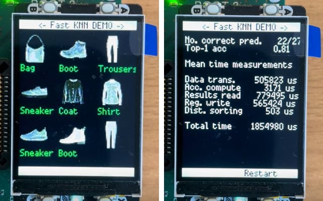
The evaluation environment for nanoSoC based fabricated ASIC die uses a low cost test board that aims to mirror the design verification environment, simplifying adoption and extension for any project. The board uses two inexpensive RP2040 chips. One provides a Serial Wire Debug (SWD) and UART debugger interface, used to monitor internal status and debug nanoSoC system. The other configures and interfaces to the nanoSoC system. The RP2040 PIO interfaces allow for custom data transfers, enabling communication via the FT1248 interface of nanoSoC to load code and data from the micro-SD Card or to display results and measurements of system performance via a small LED screen.
Reference Design Comparison Table
This table will let you compare this reference design with others on SoC Labs| Title | nanoSoC | milliSoC | megaSoC |
|---|---|---|---|
| Class | Entry | Mid Range | High End |
| Reference Design | nanoSoC | milliSoC | megaSoC/Corstone 1000 |
| Staffing | Single student / academic | Academic + dedicated post-doc | Academic Team |
| Time Scales | 6 months to 1 year | 1+ years | 18 Months - 3 Years |
| Model Forms | small | Real Time | Full Video/Large AI Model |
| Tape Out / Package and Board Costs | From 10k Euro | 25k-50k EUR | >50K - >>50K |
| Processor(s) | M0 | R5 | A53 |
| Processor(s) (speed) | <250 Mhz | 250-800 MHz | 1 GHz |
| Data Rates / On Chip Comms | <2.5 Gbps | 10-80 Gbps | >100 Gbps |
| Data Rates / Off Chip Comms | <50 Mbps | 0.1 - 0.8 Gbps | >1 Gbps |
| On Chip Memory Requirements | 32KB to sub MB | 2 MB+ | 4 MB+ |
| Virtual Prototype Environment | Xilinx ZCU104 | Arm MPS3 | HAPS |
| Tape Out Node | 65nm | 28nm | 16nm |
Related Projects and Workflows
This section details the following: the core reference design, the initial project that led to the definition of the reference design, and any additional projects that extend the reference design for new or additional applications. It also defines the related example workflows for the front end Architectural and Behavioural design stages, and the back end Logical and Physical design stages. Front end Behavioural design are usually accomplished with FPGA environments and tool chains, back end Physical design requires technology specific design rules and EDA tool suites.

 David Flynn
The aim of this project is to define a mixed signal subsystem for the nanosoc reference design.
The mixed signal subsystem should be able to sample analog signals at a regular sampling rate, and transmit a digital representation of this signal to the rest of the nanosoc system. In order to interface with real-world signals in a digital System on Chip ("SoC"), an analog to digital conversion ("ADC") is needed.
 Daniel Newbrook
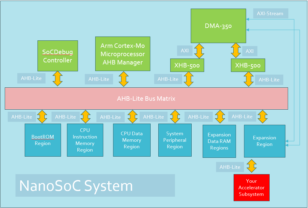
The integration of the DMA350 into the nanosoc re-usable SoC architecture improves the transfer bandwidth on DMA channels within the SoC. This project integrates the DMA 350 into nanosoc, validates the integration and functionality of the DMA 350, and compares the performance of the DMA 350 to the PL230, the first DMA controller integrated into nanosoc.
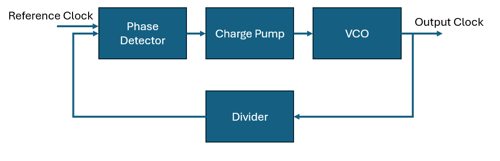
To design and verify a simple PLL for use as generator of clock signals in System on Chip design. The desired outcome from this project should be the following:
Clock generation for frequencies between 60 MHz and 1.2 GHzInclude PLL-lock signal for system start upLow clock uncertainty below 5% (transition time and jitter)Integer clock divider which can be updated at run timeMinimal areaThe resulting IP for these component blocks will be made available to the soclabs community for the upcoming design contest.
Performing system-level verification on a System-on-Chip (SoC) design is crucial for ensuring the correct function and overall performance of the entire system, rather than individual components. This project is aimed at developing the necessary resources and design flow stages for the verification of the NanoSoC reference design.
Architectural Design: Verification MethodologyWith NanoSoC, there are multiple options for performing system-level verification.
 David Mapstone
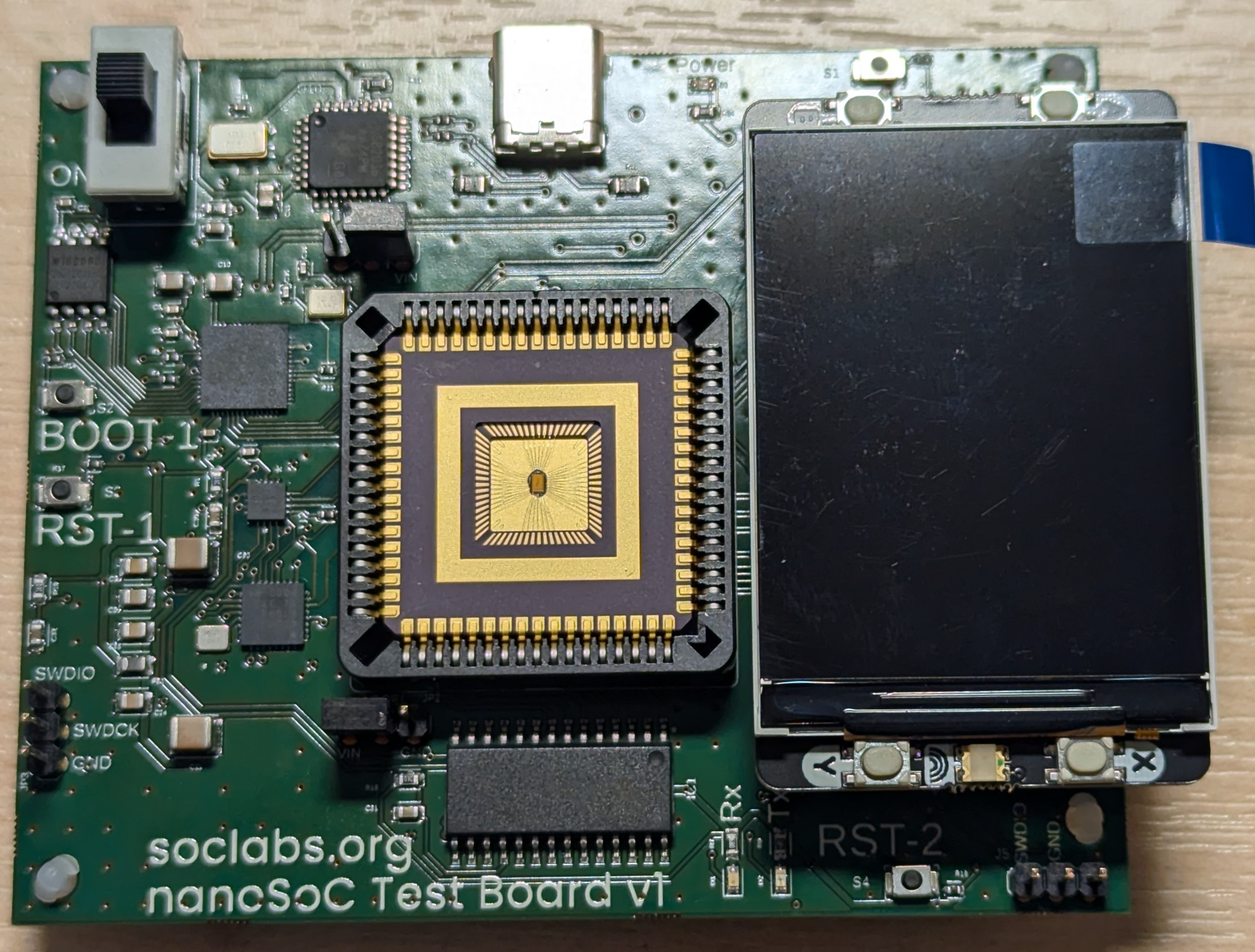
A physical test environment is required for ASIC devices fabricated following tape out. The nanoSoC test board provides a complete test environment for ASIC designs based on the nanoSoC reference design and enables the showcase of any custom designs that utilise it. Reviewing the function of nanoSoC identifies a number of design criteria for the test board:
Add new comment
To post a comment on this article, please log in to your account. New users can create an account.