PCK600 Integration in megaSoC
The PCK600 Arm IP provides components to allow a power control infrastructure to be distributed in a SoC in order to make a design energy efficient. Arm provide the IP as part of their Power Control System Architecture that can be used to control the power states of various parts of the system. This control of the power infrastructure is achieved through the use of the Power Policy Unit (PPU). This unit has an APB interface to allow for software control, and some low power interfaces that can connect to the power controllable IP within the system. A Power Control State Machine (PCSM) is responsible for controlling the physically switches and/or retention cells in the final silicon design.
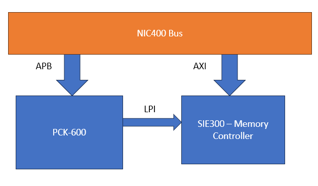
In this project, the PCK600 is being used to control the power state of the SIE300-SMC, an AXI5 memory controller from Arm. In megaSoC, these SMCs are used as AXI interfaces to the ROM and SRAMs in the system. The first integration explored here is to the ROM. This has been chosen as in theory, after bootup the ROM is never accessed again and can be completely powered down, as the system should now not be concerned with the retention state of the ROM as it is non-volatile memory.
The project will explore from Architectural Design to power aware behavioral simulations. The rest of the design flow (logical simulation to ASIC implementation) will be covered in the main megaSoC project. The goal of this project will be to successfully control the power states of the SIE300-SMC, and implement power aware simulations using a UPF file which can later be used for the power structure in megaSoC
Architectural Design
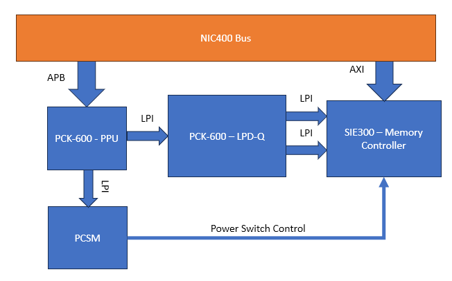
The main architecture for this subsystem is shown above. The NIC 400 is used to control the bus interfaces to the PCK600-PPU and SMC. In the Arm Power Control System Architecture, the Q-channel interfaces enable communication from sub-system parts of the SoC to the power controller and the P-Channel interface enables communication from the power controller to parts of the system that manages sub-system power states. The PPU is configured to run as a single q-channel controller. However the SIE has 2 q-channel interfaces: 1 for clock control and 1 for power control. The PPU could be configured to have 2 q-channel connections however, the sequence of these 2 q-channel interfaces is important. Because of this, a LPI q-channel distributor is used to properly sequence the 2 q-channels.
*note: the SIE300 actually has 3 q-channel interface. An extra one is used to clock gate between the SMC and the ROM, however in this project a connection of the same qreqn signal is used from the power q-channel interface to this connection as to slightly simplify the implementation as it only needs to implement full ON and full OFF states.
Behavioural Modelling
Initial behavioural modelling of the subsystem will involve testing the power control without any power aware simulation. This will verify that the PCK600 PPU can successfully turn the SMC on and off. The PPU is configured to default to the ON state on power up, so the test will first set the dynamic power state to OFF, then perform a read on the SMC AXI port (which should be allowed as the SMC should send a request to the PPU to be turned back on), then turn the SMC back ON again.
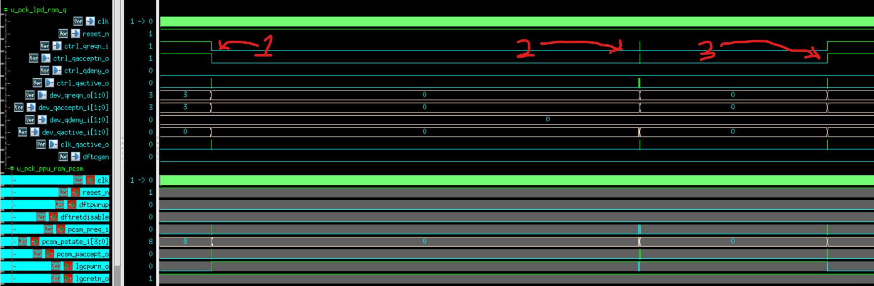
You can see from the above image. Before time-point 1, the SMC is in the on state. At time-point 1, the qreqn signal goes low, signaling a transition to the OFF state. At time point 2, an AXI read occurs on the SMC and the qactive signal requests to the PCK that it puts the SMC in the ON state, after which it goes back into the OFF state. At time-point 3, the SMC is turned back on.
Project Milestones
Do you want to view information on how to complete the work stage ""
or update the work stage for this project?
-
Architectural Design
Design FlowCompleted DateResult of WorkPCK 600 to SIE 300 architecture complete
-
Getting Started
Design FlowCompleted DateDecide on the project goal
-
IP Selection
Design FlowCompleted DateChose IP relevant for this design
Result of WorkPCK600 for power controller, SIE300-SMC for memory controller and NIC400 for bus
-
Behavioural Design
Design Flow
Team

 Daniel Newbrook
Digital Design Engineer
at University of Southampton
Research area: IoT Devices
ORCID Profile
 PCK-600 Power Control Kit
![]() Low power design
Low power design
![]() Behavioural Modelling
Behavioural Modelling
Submitted on
Comments
Power control infrastructure in Version 1 of megaSoC
Hi,
This project looks like a part of the Power control infrastructure needed for megaSoC. Can we make our plans for version 1 of megaSoC in relation to Power control infrastructure a bit more explicit?
John.
Add new comment
To post a comment on this article, please log in to your account. New users can create an account.