3D-stacked cortex-M0 SoC with wireless inter-tier data and power transfer
This project developed a 2-tier 3D-stacked Cortex-M0 SoC, in 65nm CMOS technology, with wireless inter-tier power and data transfer through an inductively coupled bus which achieved 20.3Gbps/mm2 data, and 7.1mW/mm2 power transfer simultaneously through a 250 µm channel. At the time of publishing it was the smallest ever reported inductive data and power link.
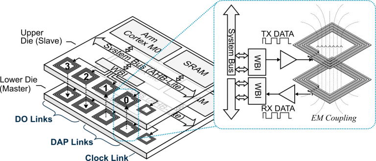
The links were integrated using a Wireless Bus Interface to implement the AHB-Lite protocol. Memory-mapped peripherals existing in separate physical dies can be addressed on the main system bus. The WBI uses a 36-bit packet structure with 4 preamble bits followed by 32 data bits. The SoC provides two Data and Power (DAP) uplinks, two Data Only (DO) downlinks, and one Clock Link (CL) to forward the clock from the lower (master) die to the upper (slave) die.
Two identical dies were stacked in a Face-to-Back (F2B) arrangement with a lateral offset of 400 µm (to align the TX and RX channels). Standard wafer-thinning to a thickness of 70 µm, resulted in a total communication distance of 80 µm including the epoxy adhesive used for assembly.
 John Darlington
Community lead at University of Southampton
 Cortex-M0
Submitted on
Add new comment
To post a comment on this article, please log in to your account. New users can create an account.