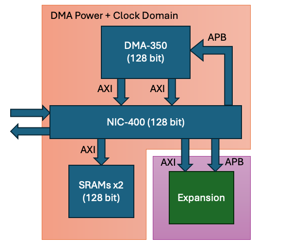
High Bandwidth Expansion Subsystem
The high bandwidth expansion subsystem is for use in systems where high bandwidth transfer to the hardware accelerator is required. This subsystem can be added to a larger SoC through the 2x full AXI ports (1 subordinate and 1 manager). This subsystem will be used in SoClabs' upcoming reference designs millisoc (a Cortex M55 based SoC) and megaSoC (a Cortex A53 based SoC).
This subsystem is available on our git here
Specification
- High bandwidth transfer to and from accelerator region (>100 Gb/s at 1 GHz)
- Wide data channel (128-bit)
- Full power control over subsystem
- DMA transfer to/from:
- Subsystem SRAMs
- Accelerator
- External system
IP Used
The HB-expansion subsystem uses:
- DMA-350
- NIC-400
- SIE-300 (SRAM controller)
Verification
CocoTB has been used to verify this subsystem. This was chosen as it can be easily used to create AXI manager and subordinate components using the cocotbext-axi libraries.
Functional verification plan:
- AXI read/write access of SRAMs
- 8/16/32/64/128 bit read/write access of SRAMs
- Read access to DMA-350 registers over APB
- DMA-350 configuration and transfer from SRAM0 to SRAM1
- DMA-350 transfer from SRAM 0 and 1 over SS AXI manager
- DMA-350 transfer from subsystem AXI manager to SRAM
With a 1 GHz clock speed for the expansion clock domain, allows for a 106 Gb/s transfer speed between the 2 SRAMs using the DMA-350
Accelerator Integration
The accelerator expansion port has both a 128-bit wide AXI port for data transfer as well as an APB port for register access and control of your accelerator.
FPGA Integration
This subsystem can be integrated directly with the processing system (PS) of an FPGA or as part of a larger SoC in FPGA. Currently scripts to build the subsystem are under development
Power and Clock control
Currently clock control interfaces are at the top level of the subsystem for the control of the clock gating in the NIC-400 subsystem bus. Further work is needed to add power and clock control to the other components in this sub-system.
Address Map
| Region | Base Address | Size | End Address |
|---|---|---|---|
| SRAM 0 | 0x60000000 | 0x40000 | 0x6003FFFF |
| SRAM 1 | 0x60040000 | 0x40000 | 0x6007FFFF |
| Expansion (AXI) | 0x60080000 | 0x40000 | 0x600BFFFF |
| DMA (APB) | 0x600C0000 | 0x2000 | 0x600C1FFF |
| Expansion (APB) | 0x600C2000 | 0x2000 | 0x600C2FFF |
| SRAM 0 (alias) | 0x68000000 | 0x40000 | 0x6803FFFF |
| SRAM 1 (alias) | 0x68040000 | 0x40000 | 0x6807FFFF |
Further Work
- Integration of P and Q-channel control to all of the sublocks to allow control of power usage
- FPGA integration
Team


 Daniel Newbrook
Digital Design Engineer
at University of Southampton
Research area: IoT Devices
ORCID Profile
 Corelink DMA-350
 CoreLink NIC-400
![]() Hardware design
Hardware design
![]() Low power design
Low power design
![]() Behavioural Modelling
Behavioural Modelling
Submitted on
Add new comment
To post a comment on this article, please log in to your account. New users can create an account.