Real-Time Edge AI SoC: High-Speed Low Complexity Reconfigurable-Scalable Architecture for Deep Neural Networks
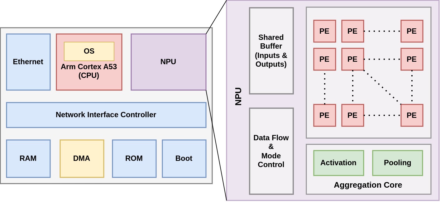
Modern Convolutional Neural Networks (CNNs) are known to be computationally and memory costly owing to the deep structure that is constantly growing. A reconfigurable design is crucial in tackling this difficulty since neural network requirements are always evolving. The suggested architecture is adaptable to the needs of the neural network. The suggested architecture is flexible enough to compute various networks with any size input image. System-on-Chip (SoC) development for this accelerator is required in order to provide a single-chip solution for CNN edge inference that incorporates preprocessing of the data and layerwise control over the inputs and outputs. The tight coupling between the accelerator and other components, such as memory interfaces and peripherals, is made possible by integrating our accelerator, also known as the NPU (Neural Processing Unit), into a SoC. This makes data movement more effective and lowers the latency, which enhances the overall performance of the deep learning tasks. Also the host processing system, such as a CPU or GPU, can be seamlessly integrated with the NPU as a result of a SoC.
Through this connection, it is possible to transfer computationally demanding Deep Learning (DL) activities to the accelerator, offloading the host CPU for other tasks and enhancing system efficiency. The advantage of future extension and upgrades is available with a SoC-based NPU. The SoC can be upgraded to include superior accelerator architectures or other hardware components to keep up with the developments in DL capabilities as algorithms and technology evolve. By using customized algorithms on CPU to fragment the image and a dedicated controller to keep track of the different scheduling tasks to be implemented on the NPU, this SoC will be able to handle a range of image sizes as inputs to the CNN, proving that it is an image-scalable and reconfigurable NPU-based SoC. Additionally, the SoC may increase its access to cloud resources with the aid of an Ethernet connector, allowing it to apply effective neural network preprocessing methods like network adaptation, post-training quantization and pruning for CNNs with billions of weights in a digital-twin setup.
Project Milestones
Do you want to view information on how to complete the work stage ""
or update the work stage for this project?
-
Design upgradtions of NPU
Target DateCompleted Date- Designing dedicated data paths for NPU's control logic, kernels, and input activation ports with AXI4-Lite and AXI4-Stream.
- Adding DMA support to the NPU for real-time data transfers from the processor and DDR memory.
- Distributed memory banks to process a higher number of feature kernels per image tile for better throughput.
- Creation of an address map in the main memory of NPU for burst transactions to enable load and fetch from the processor.
-
Unit-level verification of NPU
Target DateCompleted Date- Generation of the golden reference to build the verification benches for various test cases.
- Verifying NPU with Xilinx Vivado and Cadence Genus with layerwise benchmarking of CNN at the simulation level.
- Identification of delays (WNS/Hold) with worst paths with necessary updates in the RTL.
- Final verification of NPU with the test vectors after interface-level integration for power and area estimates.
-
FPGA Prototyping of NPU; Backend Runs of NPU
Target DateCompleted Date- Benchmarking of NPU with the CNNs for throughput and latency analysis.
- Optimization of the RTL based on the benchmark results and re-run of unit-level verification.
- Gate-level simulations of NPU with Pre- and Post-Route netlists with timing analysis.
- Reoptimization of RTL and memories with verification and FPGA prototyping.
-
Configuration of Corstone and DMA350; Development of Drivers of NPU
Target DateCompleted Date- Generation of valid configuration of corstone with pros and cons analysis.
- Out-of-Box testing of the entire SoC with Arm's Test Benches.
- Identification of integration port for NPU and DMA in the address space NIC450.
- Driver development of NPU to convert the user instructions to ISA of NPU.
- Improvement of NPU's performance with optimizations in data path from the host.
-
NPU-SoC Compiler with Neural Network Optimization
Target DateCompleted Date- Scaling down total MACs of CNN based on hardware resources available on NPU-SoC through novel model compression techniques.
- Latency improvement with reduction in data precision of input and intermediate activations.
- Performance and accuracy improvement by eliminating computations which are not important for current layer outputs through back-tracing of layer dependencies.
- We concluded that there is significant reduction in total MACs thereby lowering power consumption.
-
DMA350 and NPU Integration with SoC (with Verification)
Target DateCompleted Date- DMA350 integrated to the external system harness port of the Corstone-SSE thereby adding it to the address space of NIC450.
- Functionality verified of AXI4 Stream Channels of DMA350 in loopback mode.
- Integration of NPU with DMA350 through AXI4 Stream Channels, with functionality check with stimulus from host0 of Corstone.
- Testing is performed from the host-OCVM-NIC450-DMA350-NPU and then writing back the computed values to the OCVM.
- Entire CNN has been tested through the above mentioned method to get performance analysis.
-
Arm Cortex A53 Configuring and Synthesis
Target Date- ASIC synthesis of standalone Arm Cortex A53 (L2 Cache= 512KB) is completed.
- Area estimates has been reported as 4.9 sq. mm without using Tech Dependent cells.
- Synthesis results with TSMC 28nm Memories the area is 3.1 sq.mm and timing closed at 850Mhz (approx.)
- L1 I and D cache sizes are 32KB each.
- L2 Cache is 1024 KB
- Major challenges:
- Write Masking logic and signals has to be added to few memories, else functionality is failed.
- Write assist signal has to be handled in a correct way to avoid timing issues to get best frequency.
- Unconnected wires and few signals assigned to low causes net overlap in synthesis stage.
-
PLL Integration into SoC
Target Date- Adding APB in NIC450 using AMBA Designer for integrating PLL IP.
- Development of corresponding unit-level test cases for it with full system verification.
- Successfully booting CM0+ and CA53.
- All the tests passed which were previously conducted without PLL.
-
On-Chip Memory and External Interface Integration
Target Date- The on-chip storage is 4MB or 8MB to cater the needs of neural network computations.
- Entire memory space is divided into smaller memory instances to avoid timing issues.
- A dedicated memory translation wrapper is used for virtual to physical address mapping.
- This memory is also used for storing the CPU boot information.
- Hence the entire boot file is divided into several chunks for memcopy to the corresponding memory instances.
- External interface has been added using the DMA350 IP.
-
DRC checks, STA and Physical Design [Backend Design]
Target Date -
Tapeout
Target Date
Team


 Project Creator
 Amit Acharyya
Professor
at Indian Institute of Technology Hyderabad (IITH)
Research area: VLSI systems resource-constrained applications, Low Power Design Techniques, Machine learning hardware design, Signal Processing Algorithm and VLSI Architectures, Digital Arithmetic, Biomedical Devices. AI/ML, Nanoscience & Technology
ORCID Profile
 Cortex-A53
 Corelink DMA-350
![]() Hardware design
Hardware design
![]() Low power design
Low power design
Submitted on
Comments
On chip storage requirement
Hi,
Thanks for the latest milestones. I see "the on-chip storage is 4MB or 8MB to cater the needs of neural network computations". I was interested in how this compares to the ChipKit tape out.
That project had the following die:
With 4MB SRAM and a SoC architecture of:
Off chip coordination and communication
The original project looked to potentially use Ethernet connectivity to off load tasks to the cloud. I understand the project is looking at a simpler off chip strategy for now? Perhaps you can share where the project has got to with this aspect?
Off-Chip Communication
Yes, initially, our architecture was designed with the intention of using Ethernet connectivity to off-load tasks to the cloud. However, due to the unavailability of the necessary Ethernet IP, we pivoted to a simpler off-chip strategy. Instead of relying on cloud processing, we now store intermediate outputs and handle post-processing locally. This approach reduces our dependence on the cloud.
That said, we've included an external AXI Stream interface in our design. This interface maintains the potential for cloud connectivity in the future, as it allows us to connect to an external FPGA if needed. This setup ensures that we're not completely closing off the option of cloud-based processing down the line.
Tasks that are to run on the A53 CPU
Hi,
It would be great to know some details of the processes that are expected to run on the A53 class processor.
Reading the project the tasking seems to be:
Have you decided on the software stack requirements needed for the A53 CPU?
Use of CoreLink NIC-450
The CoreLink NIC-450 you have identified provides some Arm blocks such as QoS-400 and QVN-400 that support Quality of Service protocols for specific latency concerns and other capabilities to better manage different data flows.
You have identified data movement efficiency and latency as key issues to overall performance of your deep learning tasks. You also mention using the CPU to fragment the image. Do you see the Quality of Service as important to your design?
Welcome and an exciting project
Thanks for joining the contest and this looks like an exciting project. We look forward to seeing it develop.
Add new comment
To post a comment on this article, please log in to your account. New users can create an account.