SHA-2 Accelerator Engine
Motivation
At SoC Labs, we have need of an accelerator to test our SoC infrastructure and confirmation of our accelerator wrapper design to get size and performance information as well as to try and get ahead and uncover potential problems researchers may experience trying to put their IP into the reference SoC.
Specification
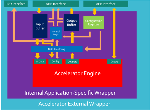
The preliminary design has been broken into two main blocks:
- Hashing channel - This is responsible for taking in input and configuration data and combining it in order to produce a hash at the output.
- Debug and validation channel - This allows a user to gain access to the accelerator and gain control over certain parts of the design (such as disabling specific hashing streams) or to gain status information and statistics from the accelerator.
This preliminary accelerator engine model is still under review and likely to change. The SHA-2 Accelerator will initially be using a 512-bit input data port, a 66-bit configuration port, a 256-bit Output data port and an X-bit Debug port.
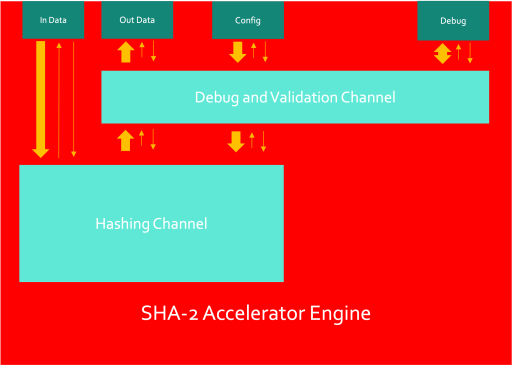
Hashing Channel
The hashing channel is comprised of a message builder and a hash compressor.
The message builder combines the 512-bit message words and converts them into 512-bit message blocks by combining the data with the configuration data - mainly slotting in the message size data into the end of the last message block. Once the data has been assembled into message blocks, it is then passed into the hash compressor.
The hash compressor performs the hash calculation function of the SHA-256 standard (the only hash type currently implemented) which is made up of a 4-state state machine. This configures the working variables, initialises the hash values, performs the hash calculation and then produces an output hash on the last message block of the data packet.
In order to support multiple hashing streams, packet schedulers will be needed to distribute packets between streams. It is not quite clear yet whether this would go between the message builder and the hash compressor or outside the hashing channel and then multiple hashing channels will be instantiated.
Debug Channel
The debug and validation channel has two main responsibilities - collecting statistical information about the accelerator and validating the order of hashes from the hashing channel. The latter is important in the case where multiple hashing channels may be instantiated. The time to hash a packet is entirely dependent on the message length so output hashes may come back out of order so ID's are assigned to packets as they enter the accelerator and the validator is responsible for re-ordering them in the order they came in. These ID's are appended to the config data as they come in before being sent to the hashing channel. The ID's are effectively invisible outside of the accelerator and are used only for internal reordering of packets if they become out of order.
The debug port can be used to access the following statistics:
- In-flight hashes - number of hashes in progress
- Hash count - number of hashes since last reset
- Current Packet ID - current ID being issued (or leaving the accelerator - tbd)
- Average Packet Size - average bit length of last 10 packets
The debug port can also be used to disable specific hashing streams to reduce power consumption, disable the entire accelerator and perform a soft reset of accelerator components.
The specification is being amended and built upon as I go and everything is under constant review. Components may move around and out of the accelerator engine and into the wrapper and I am adopting an agile approach throughout this exercise.
Implementation
Currently, a bare-bones accelerator consisting of a message builder, a couple of FIFO buffers at the inputs and output along with a hash compressor have been created. This has been basically verified but there is still a lot of work to do.
My next step is to build the debug unit and verify the behaviour of that before putting it all together and then trying to create a simple message scheduler to allow for multiple hash streams.
Verification
As mentioned in the previous section, some basic verification has been performed. I have written a python model which is able to generate input stimuli and output references to check functionality and component dynamics. This needs to be expanded greatly to cover more system control and corner cases.
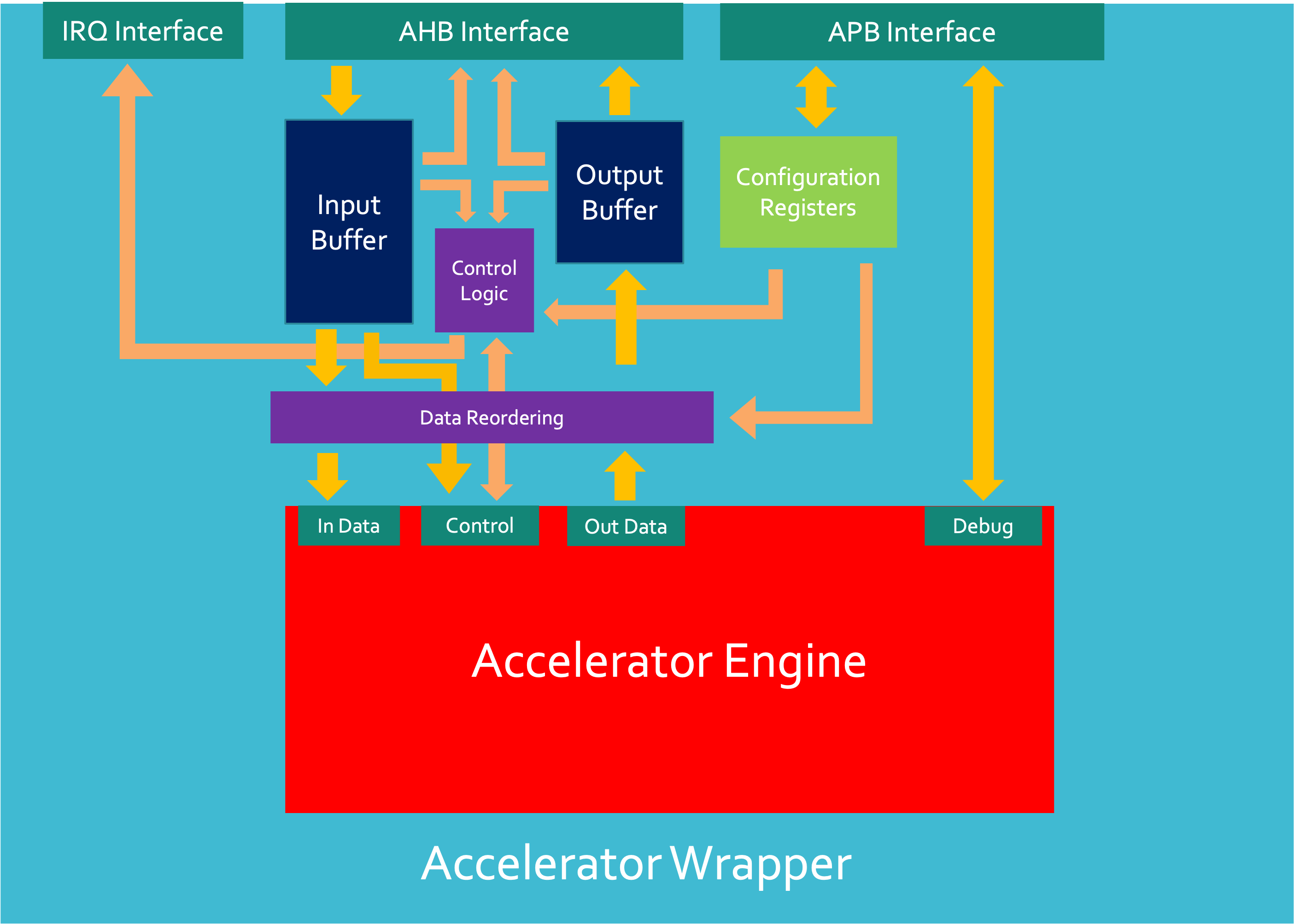
System Integration
To be able to integrate this accelerator engine into an SoC, at least one wrapper will be needed to allow the engine to interface with the system buses. This will be a seperate project of its own and I will keep this updated for when wrapper development begins.
Design Dependencies
The external interconnects that the accelerator will use to communicate with the SoC infrastructure are as follows:
- AHB interconnects - will have at least 2 memory-mapped addressed - one for reading the output buffer and one for writing to the input buffer of the accelerator wrapper. This will have a 32-bit address space and will have a 32bit (under review) data width.
- The input buffer address will have packets that require hashing
- The output buffer address will be reading the hashed values of packets in the order they were sent into the accelerator.
- APB interconnect - will have multiple memory mapped addresses - at least one for each config/control/status register in the accelerator engine plus registers in the wrapper. These will have a 32bit address width and a 32 bit data width.
- This data will be entirely dependent on the role of the control and status register in question.
- A lot of this data will be on manual request by a user on the SoC Debug interface. The user will need to either ask the Cortex M0 to perform a read of the Accelerator Debug APB port or the user will directly send an AHB (which will be translated to an APB) transaction to the accelerator wrapper to request debug data.
- IRQ interconnect - there will be at least 1 IRQ line from the accelerator to the Cortex M0 in the SoC to inform it when packets have been processed - this will likely be handled by configuration registers in the wrapper to determine the behaviour of these interrupts.
- This will likely be a 1-bit level-sensitive signal to an NVIC in the Cortex in the SoC.
The code for this project is available here and is currently under active development using a behavioural design design flow.
Team
 David Mapstone
SoC Labs Team at University of Southampton
Submitted on
Comments
Colaboration
Hello,
I am interested in collaborating in this ip design verification process. I can don this in cocotb easily.
thanks
Sana Ullah
Integration with NanoSoC?
Is this now integrated with the Wrapper and NanoSoC?
Add new comment
To post a comment on this article, please log in to your account. New users can create an account.