Implementing a UDP Echo Server using XIlinx Microblaze on a Pynq-Z2 with LAN8720 Ethernet PHY Board
Introduction
This project is evaluating the design of a simple Ethernet subsystem using the Xilinx FPGA platform.
Rationale
Part of the plans for Version 3 of nanoSoC is to expand the variety of subsystems available for the reference design. A simple, compact, open-source, Ethernet subsystem for off chip IP based communication with a low area and fabrication cost in silicon would be a useful new sub-system capability. User Datagram Protocol ("UDP"; see RFC 768) is a simple transport layer protocol within the Internet Protocol ("IP") standards to transmit messages with a minimal protocol mechanism.
In order to understand what would be required not only for the SoC Labs reference designs but also for the design flows and other project support infrastructure this project undertakes an initial design space investigation. It will give initial insight in memory sizing and core requirements to handle a full ethernet stack. The aim is for a subsystem to be developed which can be memory mapped in to existing and future reference SoC Labs SoC platforms to enable IP communication within academic projects.
The initial goal of the project is to illustrate how FPGA-based systems can implement basic Ethernet communication using a soft-core processor, programmable logic, and the Xilinx toolchain.
Implementation
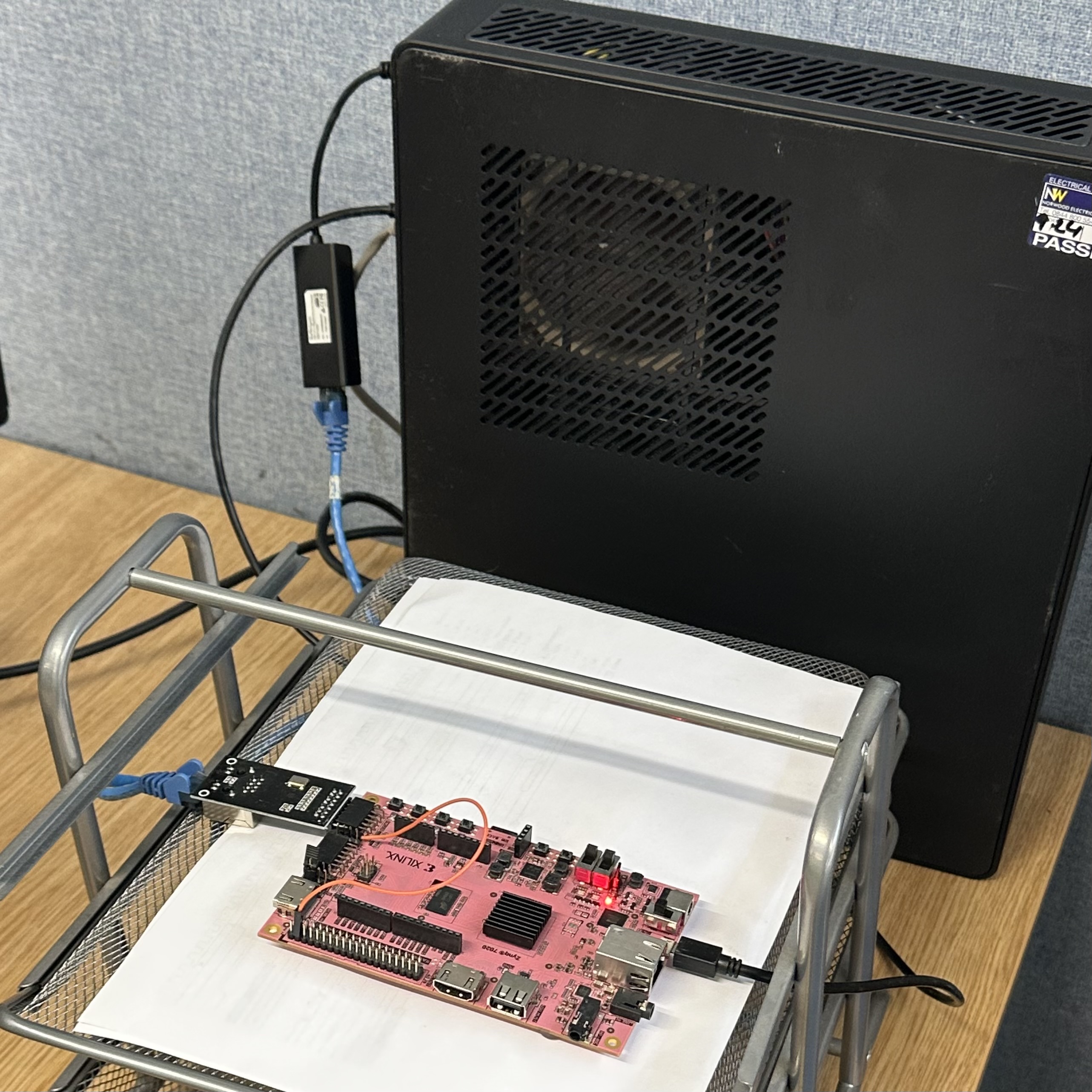
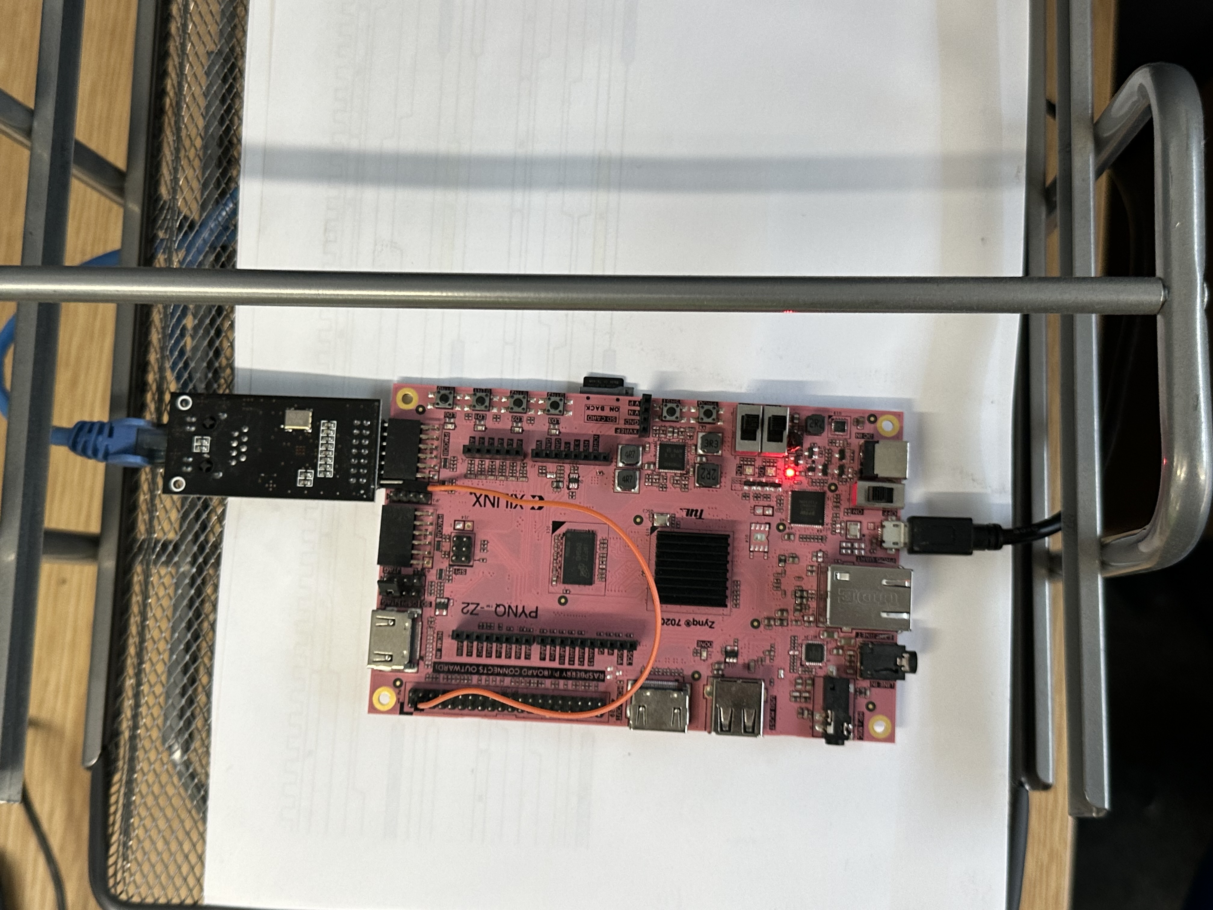
The initial design is implemented on the PYNQ-Z2 development board. For a quick start it uses a MicroBlaze soft processor with Xilinx AXI EthernetLite IP to provide a minimal but functional networking example.
The MicroBlaze processor runs embedded software that acts as the control plane for the Ethernet subsystem. Communication with the Ethernet MAC is through memory-mapped interfaces. The experimental hardware subsystem is created in Vivado using standard Xilinx IP blocks. The software running on MicroBlaze demonstrates simple Ethernet functionality such as initializing the MAC, transmitting frames, and receiving packets. Together, the hardware and software components provide a compact reference design for learning how Ethernet subsystems are constructed and integrated within Xilinx FPGA environments.
Prerequisites
Before building this example system, I have constructed a couple of test projects to lay the groundwork to get a platform that I can build off of.
UART Bridge
The first of these is a UART bridge which allows the MicroBlaze MCU to communicate with the hardened Zynq Processing Platform which will forward the UART messages both ways to make the Zynq Processing System effectively transparent. This involves configuring one of the UARTs of the PS to use the EMIO and then use the existing JTAG/UART Programmer for the usual UART interface. This reduces the need of additional hardware to communicate and means less USB devices need to be plugged in to the host. Instructions on this project and details are available here.
Ethernet PHY
Although the Pynq-Z2 has an ethernet PHY onboard, this is connected to the hardened PS and to allow for a more dynamic and representative system, I opted to purchase a LAN8720 ethernet board which has an RMII interface. This reduced pinout is important for small SoCs such as nanoSoC with a small numbers of pads which was why it was selected. Pins often constrain the size of the die on small silicon designs. I have created constraints and used the example design provided by Xilinx with an open-source MII to RMII adapter to allow for communication between the host server over a USB to ethernet adapter and the board. The packet counters can be seen and I was able to capture transactions using Internal Logic Analysers (ILAs) which proved the board had been connected correctly. Source code for this project is available here.
MII to RMII Adapter
To make my life easier and to make it more reproducible, I have created a packaged XIlinx IP which wraps the MII to RMII adapter so it can be dropped in to Vivado in a block diagram and configured that way. This uses the open source project provided by WangXuan95 on Github. The ultimate aim is to build our own adapter but this is a start to get us going. The link speed is configurable although it has only been tested at 100 with the ethboard as I haven't yet written a driver to change the link speed. Our wrapper project is available here.
System Architecture
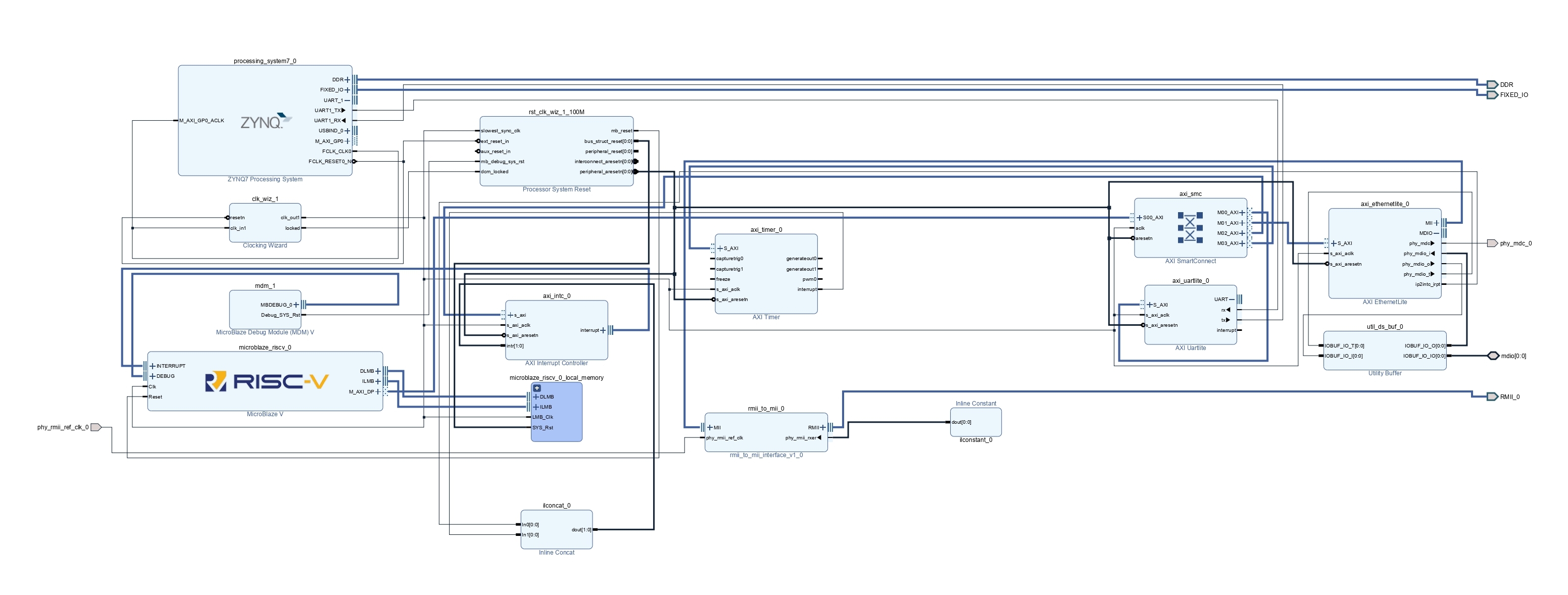
The system is built around a MicroBlaze soft-core processor implemented in the programmable logic of the PYNQ-Z2’s Zynq-7000 FPGA. The MicroBlaze acts as the main controller for the design, executing the embedded software that manages the Ethernet subsystem and other peripherals. To provide fast access to program code and data, the processor connects to dedicated local block memory through the Instruction Local Memory Bus (ILMB) and Data Local Memory Bus (DLMB). A MicroBlaze Debug Module is also included in the design, allowing the processor to be programmed and debugged directly from the development environment.
Communication between the processor and the system peripherals is handled using the AXI interconnect architecture. The MicroBlaze exposes a master AXI interface which connects to an AXI SmartConnect block. This interconnect routes memory-mapped transactions to several AXI peripherals used within the system, including the Ethernet controller, UART interface, and timer module. The AXI UARTLite peripheral provides a simple serial interface that can be used for console output and debugging, while the AXI Timer can generate periodic interrupts or be used for timing measurements within the software.
Ethernet functionality is provided by the AXI EthernetLite MAC, a lightweight Ethernet controller suitable for small embedded designs. The MAC communicates with the external Ethernet PHY using a Media Independent Interface (MII). Because the PYNQ-Z2 board exposes an RMII-based Ethernet interface, an RMII-to-MII conversion module is used to translate between the two protocols. The Ethernet subsystem also includes an MDIO management interface, allowing the MicroBlaze software to configure and monitor the PHY device.
Peripheral interrupt signals are combined using an AXI Interrupt Controller, which collects interrupt requests from devices such as the Ethernet MAC, timer, and UART. These signals are aggregated and delivered to the MicroBlaze processor as a single interrupt input, allowing the software to respond to events such as received Ethernet packets or timer expirations.
Clocking and reset control for the design are handled by a Clocking Wizard and a Processor System Reset module. These blocks generate the required system clocks and ensure that all components are reset in the correct sequence during system startup. The Zynq Processing System is included in the design primarily to provide board infrastructure such as base clock sources and access to the board’s external interfaces.
A firmware layer is then running on the Zynq Processing System to act as a UART Bridge and the MIcroBlaze is running a lwIP echo server. Together, this builds a simple system for demonstrating a basic UDP communication.
Software Application
The software for this project was developed using Xilinx Vitis, which provides a unified environment for creating applications that run on both the Zynq Processing System and soft processors implemented in programmable logic. The hardware design created in Vivado was exported as an XSA (Xilinx Support Archive) file, which contains the hardware description, memory map, and the FPGA bitstream. This XSA file forms the starting point in Vitis, where it is used to create a platform project describing the hardware resources available to software running on the system.
Within the Vitis workspace, separate domains were created for the two processors used in the design: the ARM Cortex-A9 cores in the Zynq Processing System and the MicroBlaze soft processor implemented in programmable logic. The ARM domain was configured to run a lightweight bare-metal application that acts as a UART bridge, providing a simple interface between the host PC and the embedded system through the Zynq PS UART. In parallel, a second domain targeting the MicroBlaze processor was created and configured to use the lwIP network stack. This domain provides the runtime environment required for networking functionality on the MicroBlaze.
Two separate applications were then developed on top of these domains. The ARM-based application running on the Cortex-A9 implements the UART bridge functionality, allowing serial communication with the system for debugging or interaction with the Ethernet demonstration. The MicroBlaze application implements an lwIP echo server, which listens for incoming TCP connections and returns any received data back to the sender. This provides a simple demonstration of Ethernet communication and confirms that the Ethernet subsystem is operating correctly.
During development it was necessary to increase the MicroBlaze data memory allocation to accommodate the networking application. The lwIP stack and associated example code required more memory than the default configuration, so the MicroBlaze local memory was expanded to 512 kB. To further optimise the application size, several parameters within the lwip220 Board Support Package (BSP) were tuned. Adjusting memory pools, buffer counts, and other configuration options helped reduce the overall program footprint while still maintaining the required networking functionality.
Testing
Testing the system required establishing a simple network environment in which the FPGA board could obtain an IP address and communicate with another host. A Linux machine was configured to act as a DHCP server and was connected directly to the PYNQ-Z2 board using a USB-to-Ethernet adapter which was showing as its own ethernet adapter in ifconfig. This setup allowed the board to dynamically request an IP address when the lwIP stack was initialised on the MicroBlaze processor.
During early testing, the board was not successfully communicating on the network. To help diagnose the issue, additional debugging code was added to the MicroBlaze application to implement packet transmit and receive counters within the lwIP application which were then displayed successfully over the UART bridge using a configured screen session. These counters allowed basic verification that frames were being generated by the Ethernet MAC and that the software stack was attempting to process incoming traffic. This debugging process eventually revealed that the MII-to-RMII interface block had been incorrectly configured to operate at the wrong speed, and that not all required output signals had been properly exposed in the design. After correcting the configuration and rebuilding the hardware, the Ethernet interface began operating correctly.
Once the hardware interface was functioning, Wireshark was used on the Linux host to monitor the network traffic between the board and the DHCP server. The packet capture confirmed that the lwIP stack was periodically sending DHCP discovery messages and successfully completing the DHCP exchange to obtain an IP address. Further inspection of the captured traffic showed that the board was also responding correctly to ARP requests, indicating that the Ethernet MAC, PHY interface, and lwIP stack were all operating as expected.
With the network interface validated, the final step was to test the lwIP echo server running on the MicroBlaze processor. Using the nc (netcat) utility from the Linux machine, a UDP connection was opened to port 7 on the IP address assigned to the board. Any strings sent through the connection were immediately returned by the echo server, confirming successful bidirectional communication between the host and the FPGA-based networking system.
These tests verified that the complete networking stack—from the physical interface through to the lwIP application layer—was functioning correctly. The testing process also highlighted the importance of systematic debugging at both the hardware and software levels when developing FPGA-based networking systems.
Reproducing this project
The project is available here which contains the block diagram as well as instructions on how to reproduce what has been done and the environment that was established to do this. There are scripts and tools that have been installed on the host machine that allow the DHCP and echo testing which are in the scripts directory within the repository. Following the readmes within the repo, you should be able to reproduce the design that has been built in this project.
Next Steps
Following demonstrating this working, I want to continue building this subsystem in an iterative way to allow for more learning and accessible projects but to also massively help with debug at system integration where small changes are being made at a time. This means the next steps will be:
- Reduce the size of the lwIP by fine-tuning the compile and BSP options
- Replace the Microblaze with an Arm DesignStart Cortex-M3 Processor
- Create a wrapper around an Open-source Ethernet MAC and integrate it to get it to work within a Vivado Project.
- Create a Vivado wrapper around a new version of NanoSoC with configured memory sizes
- Get system working and perform a more robust suite of validation and verification tests on the system.
- Tune the lwIP application firmware.
 David Mapstone
SoC Labs Team at University of Southampton
Submitted on
Add new comment
To post a comment on this article, please log in to your account. New users can create an account.