BlackBear : A reconfigurable AI inference accelerator for large image applications
Neural networks have enabled state-of-the-art approaches to achieve impressive results on many image processing and analysis tasks. However, while gigapixel images are gaining ground in domains like satellite imaging and digital pathology, feeding neural networks directly with these ultra-high-resolution images is still computationally challenging. With a growing number of high-resolution computer vision applications being proposed, the need for an efficient and powerful AI acceleration system targeting gigapixel images rises. To that end, we propose BlackBear, a reconfigurable AI inference accelerator for large image applications.
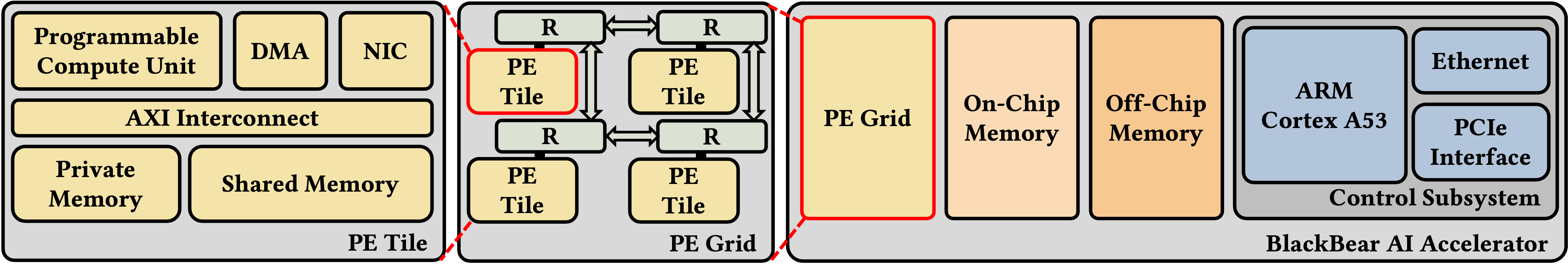
This project aims to develop a prototype for early experimentation and demonstration of crucial BlackBear features. The initial design of the BlackBear accelerator architecture consists of a grid of processing elements (PEs), on-chip and off-chip memory resources, and interconnects. The control subsystem manages available resources, orchestrates job execution, and communicates with the host through the interface. The PE grid contains 4 PEs connected by a 2x2 mesh. Each PE tile contains one programmable compute unit (a processor core equipped with matrix extension), two-piece of local memory, and other dedicated function units.
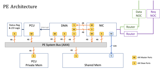
The DMA of each PE Tile is responsible for copying data between memories and external memories. The Network Interface Controllers (NICs) are designed as the bridges that exchange messages and data between PE Tiles and NoC Routers. The interfaces between PE Tiles and NoC Routers consist of several FIFOs for pushing data from one side to the other side. All interconnections between the components in PE Tiles are designed according to the AXI4 protocol.
Project Milestones
Do you want to view information on how to complete the work stage ""
or update the work stage for this project?
-
Milestone #1
Target Date -
Milestone #2
Target Date -
Milestone #3
Target Date -
Milestone #4
Target DateCompleted DateThis month, our primary focus was on defining the interfaces and interactions between the components and finalizing the microarchitecture specifications for the various blocks.
- Control Subsystem
- Draft a detailed system workflow that outlines the runtime's management of Processing Elements (PEs) within the compute grid, encompassing scheduling mechanisms and workload monitoring for efficient execution.
- Specify the file format for the Top-Level Loadable, which includes the essential network information and serves as the runtime's input.
- Implement the first runtime prototype that demonstrates the implementation of parsing the initial set of subgraphs and event handling.
- Interconnect
- Design the Data-Link Layer Protocol for messaging and data transactions on Network-on-Chip (NoCs).
- Prepare the programming interface and microarchitecture specifications for all three Network Interface Controllers (NICs) within the system. Additionally, establish a clear and comprehensive understanding of how the NICs interact with each other.
- Design and implement the NoC routers capable of supporting unicast and multicast functionalities for the two NoCs in the compute grid.
- PE Tile
- Specify the address mapping and establish interfaces between all blocks within the PE tile, ensuring seamless communication and coordination.
- Define PE-Level Loadable's file format, which contains the essential information of the dispatched model subgraphs.
- Finalize the programming interface and detailed specification for the DMA.
- Control Subsystem
-
Milestone #5
Target DateCompleted DateThis month, our primary focus was finalizing all blocks' specifications and ensuring compatibility and consistency. Additionally, we identified several system-level integration issues and proposed viable solutions.
- Control Subsystem
- Finish the Network Interface Controller (NIC) specification in the Control Subsystem.
- Cache Clusters
- Finish the specification of the Global Cache Subsystem, whose cache banks are designed as low-order interleaving to enhance the effective data throughput.
- Interconnect
- Improve the flexibility of the Data-Link Layer Protocol to support software-defined communications between different subsystems.
- Finish the Transaction Layer Protocol overlay on top of the Data Link Layer Protocol to facilitate communication among application processes running on different CPU runtimes.
- PE Tile
- Generate the Programmable Compute Unit (PCU), the system bus, and the Private Memory with third-party open-source projects.
- Finish the specification of the Shared Tensor Memory Controller for packing outbound tensors and unpacking inbound tensors.
- System Design Issues
- Large-Size Tensor Data Movement
With the Global Cache Subsystem being banked as a low-order interleaving design, the exchange and retrieval of data with cache clusters cause a significant challenge for PE-Tiles. Thus, we need to find a solution for PE-Tiles to send the correct parts of the whole tensors into corresponding cache banks. - Completion Hints Support for Tensor Write
The Control Subsystem manages the dependency of tensors between PE-Tiles. It thus needs to know if the tensor can be fetched from the cache for later computation purposes. The completion hint supports Cache Clusters to notify the Control Subsystem of such information. - Tensor ID Assignment
Our system uses Tensor ID for various purposes, such as resource management, communication, and data exchange. The finite bit length of the Tensor ID field defined in the hardware programming interfaces limits the number of on-the-fly tensors. Thus, we carefully design the Tensor ID assignment rule to prevent ID shortage.
- Large-Size Tensor Data Movement
- Control Subsystem
-
Milestone #6
Target DateCompleted Date- Verifying communication types without data exchange in Data Link Layer Protocol
- PE-Tile: Implement the Network Interface Controller (NIC), the Direct Memory Access (DMA), and a debug module acting as a PCU to finish communication procedures.
- Control subsystem: Implement a baremetal runtime running on the processor in the Processing System of our FPGA board.
- Verify hardware correctness with RTL simulation.
- Prototype the hardware design on our FPGA board and co-simulate with the runtime to monitor the process of each target communication types.
- Verifying communication types with data exchange in Data Link Layer Protocol
- PE-Tile
- Enhance the Network Interface Controller (PE-NIC), the Direct Memory Access (DMA), and the debug module acting as a PCU.
- Implement the Shared Memory Controller (SMC) to handle memory access requests from PE-Tile system bus and data copy operations through NoC interconnects.
- Control subsystem: Implement a baremetal runtime running on the processor in the Processing System of our FPGA board.
- Global cache memory: Implement the Cache Network Interface Controller (Cache-NIC) and cache controller to accept requests from components attached on NoCs and return corresponding response.
- The RTL verification and FPGA prototyping will be finished in the next milestone.
- PE-Tile
- Verifying communication types without data exchange in Data Link Layer Protocol
Team

 Project Creator
Assistant Professor
at National Cheng Kung University
Research area: computer architecture
 Cortex-A53
Submitted on
Comments
Target technology node
Hi,
Have you decided on a specific technology node as your physical target?
John.
Interconnect design
Can you give a little more detail on the specific NIC, AXI interconnect and DMA infrastructure you are intending to use?
Interconnect design
Thanks for the update on the Project milestone, that is very helpful. If you could respond the this comment with a little more specifics on the proposed specification for the DMA implementation that would be helpful. We are currently working on an additional DMA implementation for our reference design using the new DMA350 ip from Arm.
Interconnect design
Our DMA is mainly custom designed to meet our system requirements. The interfaces include direct connection to NIC, AXI bus interface, and interrupt interface to the PCU. The DMA will support data copy among external memories and PE local memories, message passing among external/PE internal CPUs, and interrupt among external/PE internal CPUs.
Use of Network Interface Controllers
Hi,
Could you explain which Network Interface Controller IP you are using.
John.
Add new comment
To post a comment on this article, please log in to your account. New users can create an account.