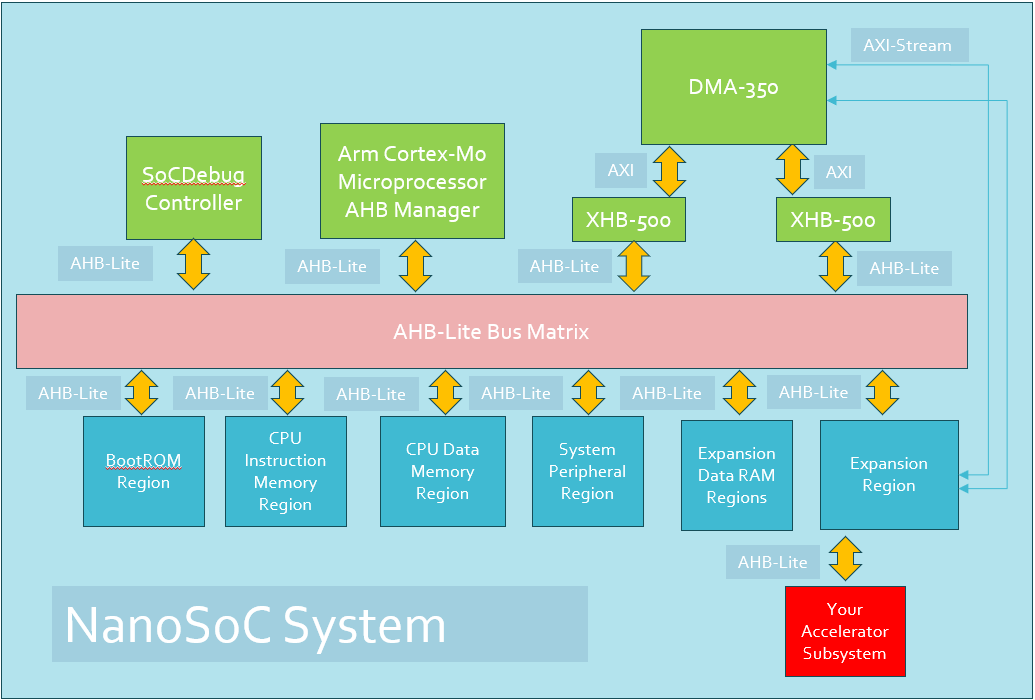
DMA 350 integration with nanoSoC
The integration of the DMA350 into the nanosoc re-usable SoC architecture improves the transfer bandwidth on DMA channels within the SoC. This project integrates the DMA 350 into nanosoc, validates the integration and functionality of the DMA 350, and compares the performance of the DMA 350 to the PL230, the first DMA controller integrated into nanosoc.
Configuring the DMA
The DMA 350 has options for configuration, these include: bus data & address widths, number of channels, number of input/output triggers, number of stream interfaces, number of GPOs, the use of an additional AXI master port and the use of TrustZone security. All these optional features come with tradeoffs in power and area. To keep the area to a sensible size for a nanosoc implementation we have configured the DMA as follows:
| Feature | Value |
|---|---|
| GPO_width | 1 |
| No. of channels | 2 |
| Stream interfaces | 2 |
| Channel FIFO depth | 32 |
| Triggers in | 2 |
| Triggers out | 2 |
| AXI M1 present | Yes |
| TrustZone | No |
With this configuration, each of the 2 channels has stream and trigger interfaces. It can also use a different AXI master for each channel, or use both AXI masters on a single channel. With choice of FIFO depth, some tests were done with different FIFO depths and a transfer size of 256 and the results are as follows:
| FIFO depth | Normalised bandwidth |
|---|---|
| 2 | 1.00 |
| 4 | 1.55 |
| 8 | 2.14 |
| 16 | 2.61 |
| 32 | 2.89 |
| 64 | 2.89 |
The 32 deep gives the best performance, and increasing any further does not see any change for this transfer size at least.
AXI to AHB
Arm provide the XHB-500 for AXI to AHB conversion. The configuration for this is relatively minimal, just ensuring the data and address widths are consistent, and the ID widths are correct for the configuration of the DMA-350. The XHB-500 uses AXI5 - AHB5, but nanosoc is an AHB lite system. To achieve this conversion, the hnonsec, hexcl, hqos, hregion, and hnsaid can be ignored. The hexokay signal must be tied to 0.
The AHB signals from the sldma350_ahb.v module are then connected into the nanosoc_ss_dma.v module. To still allow for users to chose between PL230 and DMA-350, some defines are used. This allows the choice between 1x DMA-350, 1x PL230 or 2x PL230 (set by DMAC_DMA350, DMAC_0_PL230, DMAC_1_PL230)
Changes to nanoSoC
To allow the integration of the DMA350 into nanoSoC, the APB address map had to be altered. Until this point all the APB completers required 12 bit address widths, where the DMA350 requires 13 bit addresses. To accommodate this extra space the DMA350 spans 2 APB regions. The changes are highlighted in the address map below:
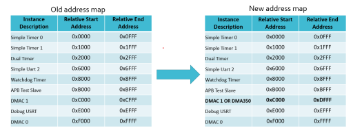
The sysctrl address space is offset to 0x40000000. With the DMA 350 at 0x4000C000 - 0x4000DFFF
Some additional changes were made to allow the use of stream interfaces. These interfaces are passed to the expansion space so they can be used by your accelerator.
Validating the integration
To validate the functional behaviour of the DMA-350 within the nanosoc test code has been written for the Cortex M0 to run. The tests currently included are:
- 1D transfer from EXPRAM0 to EXPRAM1 with interrupts
- 1D transfer from EXPRAM0 to EXPRAM1 without interrupts
- 1D transfer from EXPRAM0 to EXPRAM1 without interrupts, and disabling burst transfers
- 1D transfer from EXPRAM0 to EXPRAM1 without interrupts, using M1 AXI interface
- 1D transfer from EXPRAM0 to EXPRAM1 without interrupts, using software triggering
Additional test include, the use of both M0 and M1 together, and the hardware triggering interface. To use the M1 interface the memory must be addressed at an offset of 0x08000000.
Performance
To compare performance between the DMA350 and PL230 tests with 64 x 32 bit transfers on both and measured the transfer time in simulation were undertaken. These used 4 different permutations of DMA transfers, firstly the PL230 as provided from ARM, secondly an upgraded version of the PL230 - this version includes caches for the source destination and control registers in the PL230 which avoids having to fetch data from the DMA data structure as often. Next with the DMA350, one permutation using just a single AXI master, and another using 2 masters.
| DMA Version | Cycles for 64 transfers | Bandwidth (Gpbs) |
|---|---|---|
| PL230 (ARM) | 388 | 0.53 |
| PL230 (SoCLabs) | 150 | 1.37 |
| DMA350 1xAXI | 130 | 1.58 |
| DMA350 2xAXI | 70 | 2.93 |
The soclabs PL230 version outperforms the ARM version, this is because in the default ARM supplied version of the PL230, the dma first fetches information for the source and destination from the DMA data structure, then performs a single read and single write, it has to repeat this for each word transferred. In the soclabs version, it creates a cached copy of the transfer information and then performs 16 read-write cycles. This gives a significant enhancement as it does not have to fetch data from the DMA data structure as often.
The DMA350 however, has an internal data structure so does not have to fetch any information whilst running. It also has FIFOs for each channel and so can do sequential reads followed by writes rather than doing single read-writes as the PL230 does. This gives about a 15% enhancement in bandwidth, however the DMA350 does have a significantly larger synthesizes area (about 30x larger than the enhanced PL230). The best performance comes from using both of the AXI masters. Because nanosoc has a 4x7 bus matrix, each master effectively has its own bus, meaning reading and writing can happen concurrently. This gives over 100% increase in bandwidth compared to the enhanced PL230, and 85% increase compared to the DMA350 with a single master.
Using the DMA350 in your project
Currently, the default option for DMA in nanosoc is the enhanced PL230. If you would like to use the DMA350 in your project. You can include this by adding the DMAC_DMA350 definition to NANOSOC_DEFINES in the makefile in nanosoc_tech. This will replace the PL230, you cannot instantiated both at the same time. You will also need to include the DMA350 ip in the system level flist (accelerator-project/flist/system.flist). This can be done by uncommenting the line including the sldma350_ahb.flist. It is suggested that the sldma230_ip.flist is commented out to avoid the inclusion of that IP in simulation etc.
There are some drivers provided for testcode development in the nanosoc_tech/software/drivers/ directory, and nanosoc_tech/software/common/validation/dma350_tests.c is provided as a baseline for firmware development
Adapting interrupts
The default interrupt map for the nanoSoC can be found here. The default setup for interrupts from the DMA to the CPU is to combine any of the DMA interrupts into 1 signal. However, the DMA-350 supports interrupt signals from all of it's channels. This means the default interrupt setup would result in the same interrupt ocurring for any of the DMA channels. This may be fine if your application only has one channel running at a time (for instance if you are using 1 to load data to your accelerator and 1 to read off data). However if concurrent transfers are required it may be useful to seperate them.
In order to achieve this, override the interrupt signals from the accelerator region as currently there are a total of 4 signals from the accelerator to the CPU interrupt handler. In order to make these changes, edit the nanosoc_system file to achieve this. By changing the number of EXP_IRQ wires connected to the accelerator region, and then assigning some of the EXP_IRQ wires to the DMAC_0_DMA_DONE wires. For example; 3 channels you would:
assign EXP_IRQ[2:0] = DMAC_0_DMA_DONE[2:0];
Ideally make changes in the software to reflect this; edit the names of the interrupts in the CMSDK_CM0.h file from EXP0_IRQn to DMA0_IRQn etc.
Similarly, change the name of the interrupt handlers in the startup_CMSDK_CM0.s file from EXP0_Handler to DMA_CH0_Handler, change this for the DCD, EXPORT, and definitions to make sure the compiler can link your code to these definitions.
Then in your code you can include the interrupt handlers, for instance:
void DMA_CH0_Handler(void){
  __disable_irq();
  AdaStatType ST = AdaReadStatus(ch, SECURE);
  if (ST.STAT_DONE == 1) {
    AdaClearChDone(0, SECURE);
  } else if (ST.STAT_ERR == 1) {
    AdaClearChError(0, SECURE);
  } else if (ST.STAT_DISABLED == 1) {
    AdaClearChDisabled(0, SECURE);
  } else if (ST.STAT_STOPPED == 1) {
    AdaClearChStopped(0, SECURE);
  } else {
    printf("Unknown IRQ on CH%d!\n", 0);
  }
  dma_done_irq_occurred++;
  __enable_irq();
  return;
}
Team


Additional Project for:
 Daniel Newbrook
Digital Design Engineer
at University of Southampton
Research area: IoT Devices
ORCID Profile
 Corelink DMA-350
CoreLink DMA-230
Submitted on
Add new comment
To post a comment on this article, please log in to your account. New users can create an account.