An Efficient Hardware-based Spike Train Repetition for Energy-constrained Spiking Neural Networks
In the context of Industry 4.0, handwritten digit recognition plays a vital role in numerous applications such as smart banking systems and postal code detection. One of the most effective approaches to tackle this problem is through the use of machine learning and neural network models, which have demonstrated impressive accuracy and adaptability in visual pattern recognition tasks. However, most conventional neural networks require significant computational resources and power consumption, which pose challenges for integration into compact, low-power devices such as edge devices or embedded systems. To address this limitation, our project adopts Spiking Neural Networks (SNNs)—a brain-inspired neural model that leverages discrete, spike-based communication for information processing.
Our target is to implement a compact and low-power System-on-Chip (SoC) for real-time handwritten digit recognition using SNNs. The key innovation of this project is the Repetitive Spike Train (RST) technique, which reuses spike train outputs across time steps to reduce redundant computation and memory access—two dominant sources of energy dissipation in SNN systems.
We begin with the selection of the MNIST dataset and define an SNN model to balance accuracy and hardware efficiency. Simulation in MATLAB demonstrates that applying RST to early network layers can maintain or slightly improve accuracy (up to 98.05%) while offering compression and energy savings. Next, we identify required IPs for the NanoSoC platform, including a Cortex-M0 core, DMA, code/data SRAM, UART, ADP, and our custom RST SNN IP. These components communicate via the AHB-Lite bus.
The RST SNN IP architecture is defined with dedicated SRAMs for spike trains and synaptic weights, a spike-to-digit converter, and a Spiking Neural Processing Core controlled via an AHB interface.
In later milestones, the RTL design will be integrated into NanoSoC, and prototype validation will be performed using an FPGA. This project lays the foundation for future low-power neuromorphic chips aimed at real-time AI processing in embedded and edge systems.
Project Milestones
Do you want to view information on how to complete the work stage ""
or update the work stage for this project?
-
Getting Started
Design FlowTarget DateCompleted DateProject management
This project will follow a standard SoC development workflow, serving as a foundational element for the NanoSoC reference platform. Although it may not proceed to full tape-out or silicon validation, the project will have milestones to ensure steady progress. Each milestone will be tracked with corresponding completion dates and documentation.
To maintain agility and responsiveness, flexible intermediate goals will be established. These will help break down the overall objective—designing an energy-efficient RST-based SNN IP for handwritten digit recognition—into manageable phases, from algorithm modeling to RTL implementation and system integration.
Design methods
The project will adopt a top-down design methodology:
Algorithm Modeling: RST (Repetitive Spike Train) algorithm will be first modeled in MATLAB to simulate spiking behavior and validate the effectiveness of temporal reuse.
RTL Design: Once validated, the algorithm will be translated into synthesizable Verilog RTL as the RST SNN IP, incorporating AHB slave interface logic.
Verification & Integration: The IP will be verified using cocotb testbenches and then integrated into NanoSoC via the AHB expansion interface.
Target Implementation: Although full physical implementation is not required, synthesis using TSMC 65nm libraries will be conducted to evaluate area, power, and timing.
Access to IP
Access to standard IP blocks (Cortex M0+ core, AHB interfaces, memory, DMA) will be provided through the nanoSoC platform, while the RST SNN IP will be developed in-house.
Git to nanoSoC repository: SoCLabs / NanoSoC Tech · GitLab
Git to RST SNN IP repository:
-
data model
Design FlowTarget DateCompleted DateIn this milestone, the dataset and initial SNN architecture for handwritten digit recognition are defined. The MNIST dataset is selected due to its wide use as a benchmark for image classification tasks and its suitability for validating lightweight neural architectures on resource-constrained platforms.
The chosen SNN model consists of four layers:
- Input layer with 784 neurons (corresponding to 28×28 pixel grayscale images).
- Two hidden layers with 256 neurons each, enabling sufficient representational capacity while keeping hardware costs moderate.
- Output layer with 10 neurons, each representing one digit class from 0 to 9.
The structure is designed to balance classification performance and hardware efficiency, laying the groundwork for implementing the RST optimization in future milestones.
-
IP Selection
Design FlowTarget DateCompleted DateIn this milestone, the IPs required to build the nanoSoC platform are identified. These IPs provide the computational core, memory hierarchy, communication interfaces, and system peripherals needed to support the integration and operation of the RST SNN IP.
The SoC will include the following IPs:
Arm Cortex-M0 + SWD: A lightweight, low-power 32-bit processor core for general-purpose computation and control, with Serial Wire Debug (SWD) support for on-chip debugging.
Boot Monitor: Responsible for initial system bring-up, configuration, and test routines during boot-up.
Code SRAM Bank: Memory block dedicated to storing program instructions.
Data SRAM Bank: A separate memory block used for storing runtime data and intermediate results.
DMA Controller (PL230): Provides efficient memory-to-memory or memory-to-peripheral data transfer with minimal CPU involvement.
RST SNN IP: Custom hardware accelerator implementing the Repetitive Spike Train technique for energy-efficient spike-based inference.
Internal Interface – AHB-Lite: The AMBA AHB-Lite bus is used to interconnect the processor, memory, peripherals, and accelerator IPs for low-latency, high-throughput communication.
System Peripherals:
FT1248 Interface: Used for high-speed communication with external systems, e.g., for data input or debugging.
UART: Universal Asynchronous Receiver/Transmitter for serial communication.
GPIOs: General-purpose input/output pins for controlling external components or signaling.
This set of IPs is selected to ensure compatibility, scalability, and low power operation while meeting the functional requirements of handwritten digit recognition using SNNs
-
Specifying a SoC
Design FlowTarget DateCompleted Date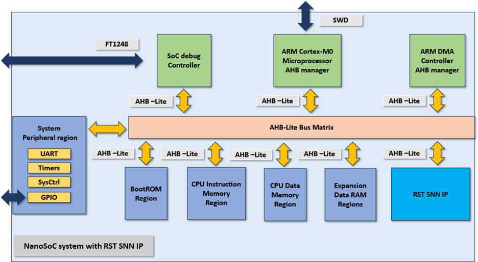
Figure 1. The overview of the architecture for nanoSoC with SNN IP
This milestone focuses on defining the overall architecture of the NanoSoC system, integrating both general-purpose components and the custom RST SNN IP accelerator. The SoC architecture is centered around a lightweight Arm Cortex-M0 processor, with system-level connectivity managed via the AMBA AHB-Lite bus.
Key components and architectural decisions include:
Processor Core: The Arm Cortex-M0 serves as the main controller, responsible for orchestrating data movement, configuration, and managing the inference flow.
Memory Subsystem: Two separate SRAM banks are implemented — one for code storage and one for data — enabling parallel access and efficient memory utilization.
RST SNN IP: The accelerator is memory-mapped and connected via AHB-Lite, allowing the processor to configure it through registers and trigger inference operations. It performs handwritten digit recognition using spike-based processing with reduced energy consumption.
DMA Controller (PL230): Enables efficient data transfers between expansion Data RAM regions and RST SNN IP without burdening the CPU.
System Peripherals: Including UART, FT1248, and GPIOs for debugging, communication, and control.
Boot Monitor: Manages the initial configuration and system setup upon startup.
AHB-Lite Interconnect: Acts as the backbone of the system, allowing seamless communication among the processor, memories, DMA, peripherals, and the RST SNN IP.
This modular SoC architecture is designed with flexibility and scalability in mind, enabling easy expansion or substitution of components. It also ensures low-power operation suitable for edge AI applications focused on handwritten digit recognition.
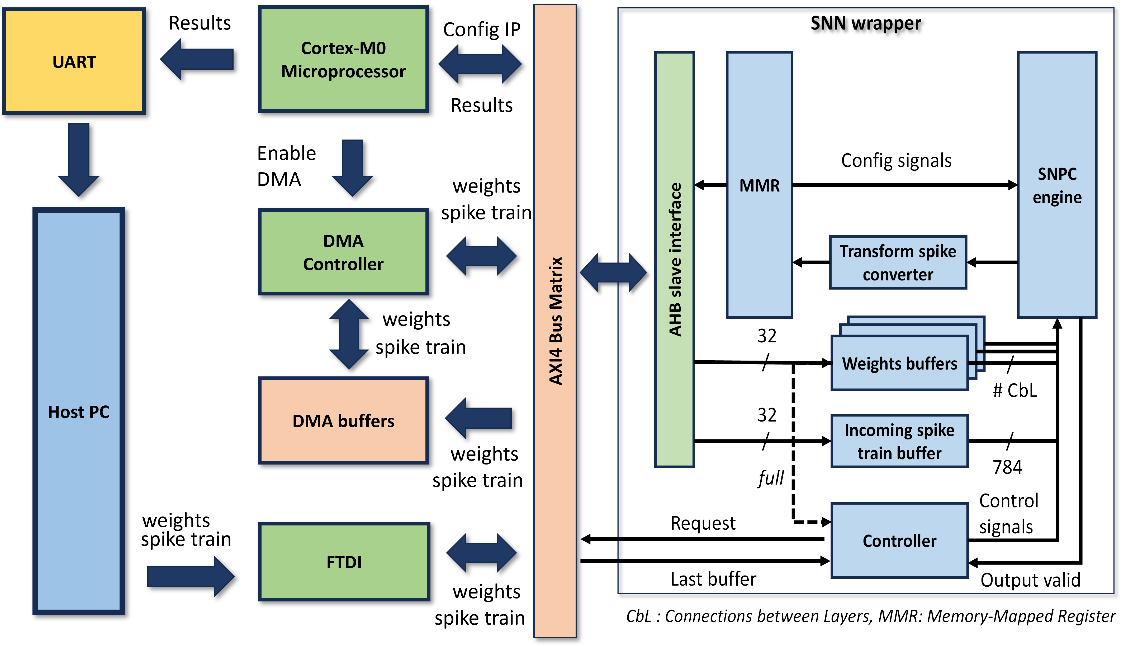
Figure 2. The details of our proposal architecture
-
Behavioural Modelling
Design FlowTarget DateCompleted DateIn this milestone, we perform a behavioral simulation of the SNN model using MATLAB to evaluate the impact of the Repetitive Spike Train (RST) method on classification accuracy. We applied the RST technique to different hidden layers across a range of Repetitive Time Steps (RTSs) from 1 to 10. The accuracy results is described in Fig. 1.
Key observations from the MATLAB simulation include:
When applying RST to the first hidden layer of SNN model, accuracy increased slightly from the baseline 97.98% to 98.05% at 3 RTSs. This shows that temporal similarity in early layers can be effectively exploited to reduce computations without degrading accuracy.
As the number of RTSs increased to 5 and 8, the accuracy dropped marginally to 97.78% and 97.76%, respectively—still within acceptable levels.
Applying RST to deeper layers (e.g., second hidden layer) resulted in greater accuracy loss due to lower spike similarity, reaching 96.03% at 9 RTSs.
When RST was applied to both hidden layers, the accuracy varied from 97.00% to 97.55%, depending on RTS configuration.
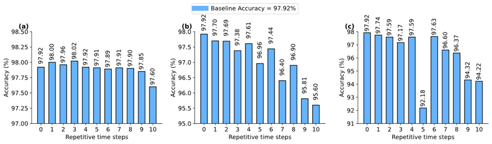
Fig. 1. Accuracy results (a) RST implementation at the first hidden layer, (b) RST implementation at the second layer, (c) RST implementation at both hidden layers.
These results validate the core assumption behind RST: temporal redundancy in spike trains, especially in early network layers, can be leveraged to improve energy efficiency without compromising classification performance. The MATLAB simulation serves as a critical foundation for the subsequent hardware modeling phase.
Result of WorkCompleted the simulation of the SNN model with RST applied, achieving maintained accuracy up to 98.05%, initially demonstrating that RST can be applied to early layers without degrading classification performance.
-
Architectural Design
Design FlowTarget DateCompleted Date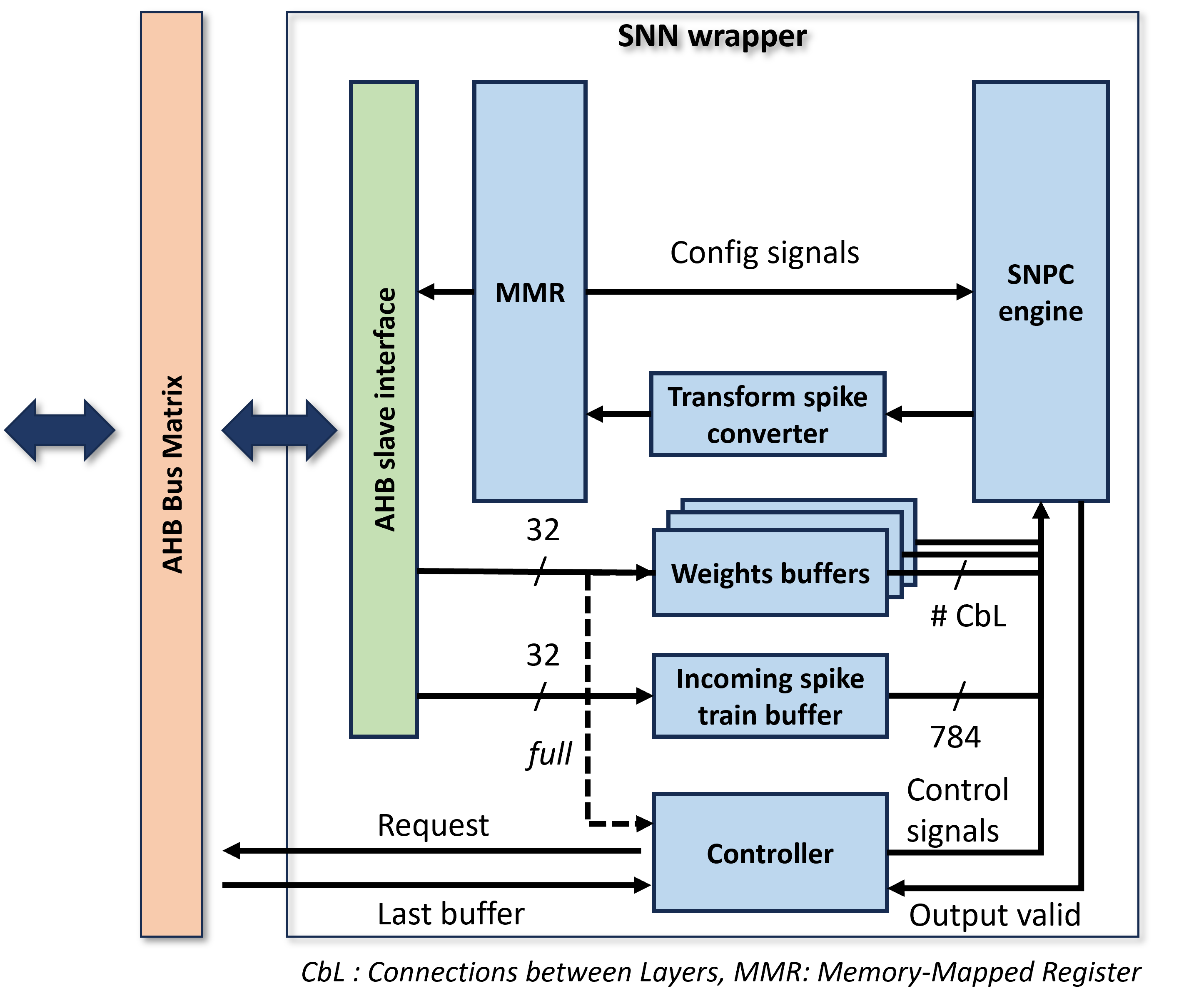
This milestone describes the finalized architecture of the RST SNN IP, a specialized hardware accelerator that executes inference using Spiking Neural Networks and the Repetitive Spike Train (RST) method. The IP is designed for integration into the NanoSoC platform via an AHB-Lite slave interface.
SNN IP's architecture (as shown in the diagram)
AHB-Lite Slave Interface
Provides the communication interface between the processor and the IP core.
Enables software to write input spike trains, configure control registers, and read final classification outputs through Memory Map Register (MMR).
Incoming spike train buffer
Stores the incoming spike trains for each time step and the first hidden layer.
Also supports temporal reuse of spikes across time steps at the first hidden layer under the RST mechanism to reduce memory access and computation.
Weights buffers
Stores pre-trained synaptic weights of the SNN model.
Accessed during inference to compute membrane potential updates in the processing core.
Weight access is minimized during repeated spike cycles to save energy.
Spiking Neural Processing Core (SNPC)
Executes the neuron-level computation based on the Leaky Integrate-and-Fire (LIF) model.
Accumulates membrane potentials, generates output spikes, and applies the RST logic to skip redundant operations.
Transform Spike Converter
Converts the final output spike pattern into a recognizable class label (e.g., digits 0–9).
Controller
Controls the data communication between SNPC and DMA PL230
-
Verification Methodology
Design FlowTarget DateCompleted DateOverview
The verification strategy for the SNN IP is divided into two primary phases:
- Block-Level Interface Verification: Using Cocotb for agile and detailed functional verification of the AHB interface.
- System-Level Integration Verification: Using the SoCLab socsim tool to validate the IP’s operation within a complete System-on-Chip (SoC) environment involving a DMA PL230 controller and software drivers.
Interface Verification with Cocotb
To ensure the SNN IP’s AHB interface strictly adheres to bus protocols, we employ a Cocotb-based co-simulation stack as illustrated in the architecture diagram:
- Python Testbench: High-level test cases are written in Python, allowing us to leverage powerful data manipulation libraries (e.g., NumPy) to generate test vectors and golden models for the SNN.
- Cocotb & VPI: The Cocotb framework manages the synchronization between the Python environment and the RTL simulator (QuestaSim) via the Verilog Procedural Interface (VPI).
Verification Flow: We developed an AHB Master agent using cocotb in Python to drive transactions (reads/writes) to the SNN IP’s configuration registers. This phase ensures that the control logic and internal registers are correctly accessible.
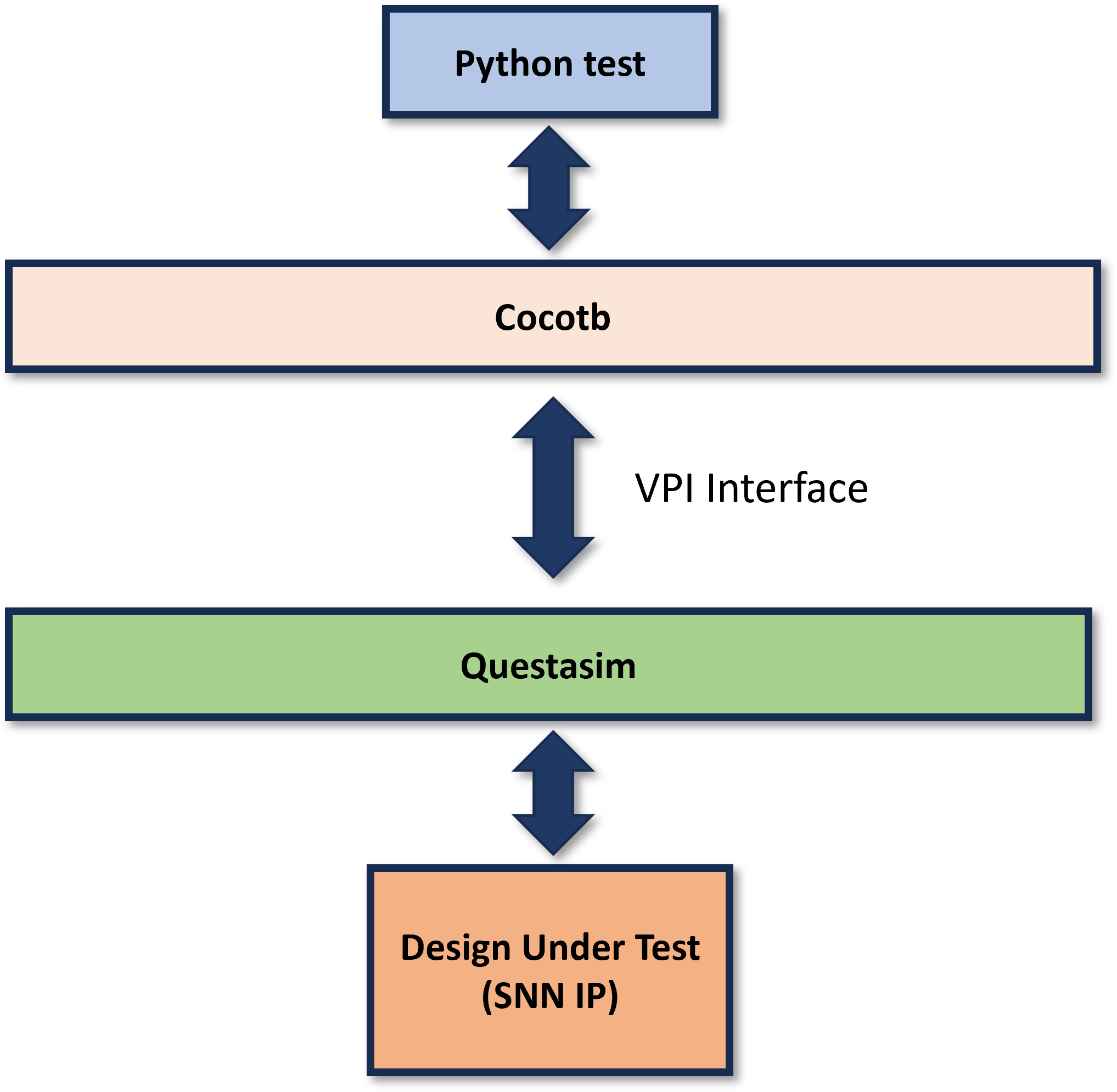
Figure 1. Cocotb testbench architecture
System-Level Simulation with socsim and DMA PL230
To verify the SNN IP’s performance and its interaction with other SoC components, we perform full-system simulation using the socsim tool provided by SoCLab.
- Hardware Configuration: The simulation environment includes the SNN IP, the PL230 DMA Controller, and a processing subsystem. The DMA PL230 is responsible for high-speed data movement, offloading the CPU from manual data transfers.
- Software-Driven Verification: We developed an embedded software program to handle the spike train preprocessing. This software converts raw neural data into a format compatible with the SNN IP's input buffer.
- The software further configures the DMA PL230 descriptors to establish a communication link, enabling the automated transfer of the preprocessed spike trains from memory to the SNN IP.
- Objectives: This phase validates the data-path integrity, interrupt handling, and the timing synchronization between the software, the DMA, and the SNN IP.
-
Generate RTL
Design FlowTarget DateCompleted DateIntroduction
The Register Transfer Level (RTL) generation phase is a critical step in transforming our architectural concepts into a verifiable digital system. For this project, we have developed a high-performance SNN IP by utilizing a modular design approach. By abstracting the hardware into functional blocks of registers and combinational logic, we ensure the design is both scalable and compatible with standard System-on-Chip (SoC) integration flows. Our RTL description serves as the foundation for synthesis, where the design is eventually mapped to physical logic gates.
SNN IP Architecture and Component Integration
The RTL of our SNN IP is composed of two primary sub-modules, representing a balance between custom high-performance logic and industry-standard connectivity:
- Custom SNPC Core (In-house RTL): The heart of the IP is the SNPC (Spiking Neural Processing Core). This block was developed in-house to implement the specific spiking neural network mathematics and neuron dynamics required for our application. The RTL defines the data flow between registers for membrane potential updates, thresholding logic, and spike generation.
- AHB Interface (nanoSoC Integration): To ensure seamless communication within a modern SoC environment, we integrated an AHB (Advanced High-performance Bus) interface sourced from the nanoSoC framework. Utilizing this pre-verified interface allows the SNN IP to function as a standard memory-mapped peripheral, enabling the CPU or DMA to configure registers and move spike data efficiently.
RTL Development Flow
The generation of the final RTL involves a multi-step integration process:
- Module Interfacing: We developed a wrapper layer to bridge the SNPC core's internal signals to the AHB bus signals (HADDR, HWDATA, HRDATA, etc.). This ensures that the custom neural logic can be controlled via standard bus transactions.
- Hierarchical Integration: The project RTL is organized into a clean directory structure that separates the core compute logic from the bus-level primitives. This modularity allows us to optimize the SNPC core independently of the interface logic.
- Synchronization: Since the design is a synchronous digital system, all data transfers between the AHB registers and the SNN compute engine are carefully synchronized to the system clock, preventing metastability and ensuring data integrity during high-speed spike processing.
-
RTL Verification
Design FlowTarget DateCompleted Date -
Simulation
Design FlowTarget DateCompleted DateIntroduction
The simulation phase serves as the definitive validation of the integrated system. By following the strategy outlined in the Verification Methodology, we executed a full-system simulation to ensure that the SNN IP, the DMA PL230, and the CPU work in perfect synchrony. This simulation verifies the entire data path, from the initial storage of neural parameters in system memory to the final inference results generated by the SNN core.
System Simulation Execution Flow
The simulation mimics the real-world operational sequence of the SoC, divided into five critical stages:
- Stage 1: System Boot & Data Initialization Upon system reset, the simulation environment loads the preprocessed spike train and synaptic weights into the system RAM. This represents the "Golden Data" prepared by our software preprocessing scripts.
- Stage 2: Processor Configuration The CPU executes the initialization code, sending AHB write transactions to configure the control registers of both the DMA PL230 and the SNN IP. In this stage, parameters such as the number of neurons, thresholds, and transfer lengths are established.
- Stage 3: Weight Loading via DMA The DMA PL230 takes control of the bus to perform a high-speed burst transfer, moving the weight matrices from the system RAM directly into the internal SRAM of the SNN IP. This verifies the IP's ability to handle DMA-driven AHB slave writes.
- Stage 4: Spike Train Streaming Once the weights are loaded, the DMA initiates the transfer of the spike train into the IP's input buffer. This stage is critical for validating the synchronization between the producer (DMA) and the consumer (SNN IP).
- Stage 5: Neural Computation & Inference The SNN IP begins the spiking neural processing. The simulation tracks the membrane potential updates and spike generations across the programmed number of timesteps. Once the computation is complete, the IP signals the end of the task, and the results are read back for verification.
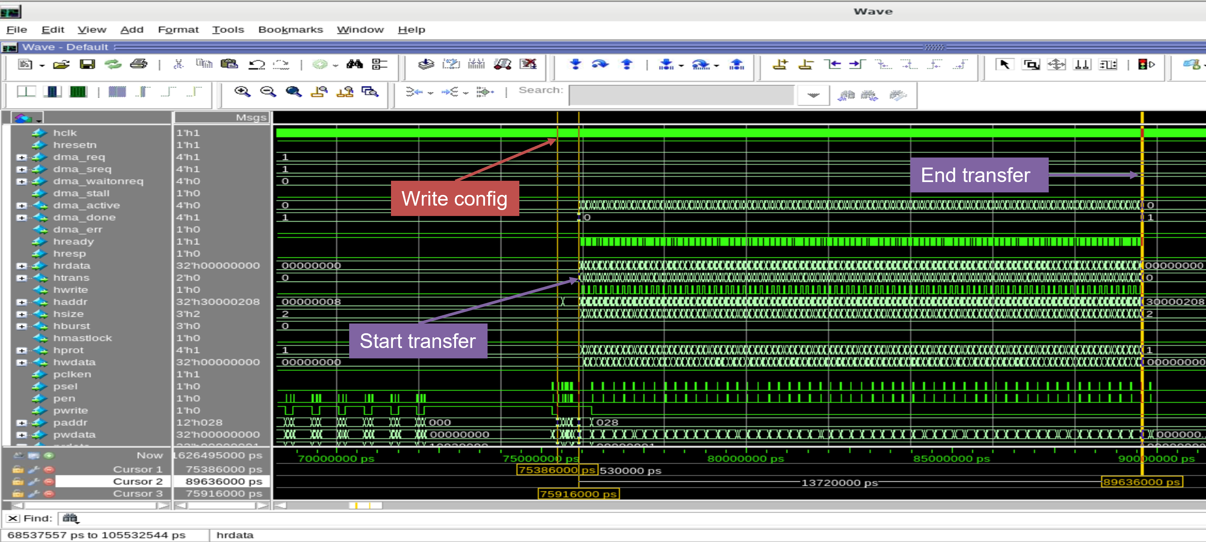
Figure 1. The configuration write transaction and weight transfer process
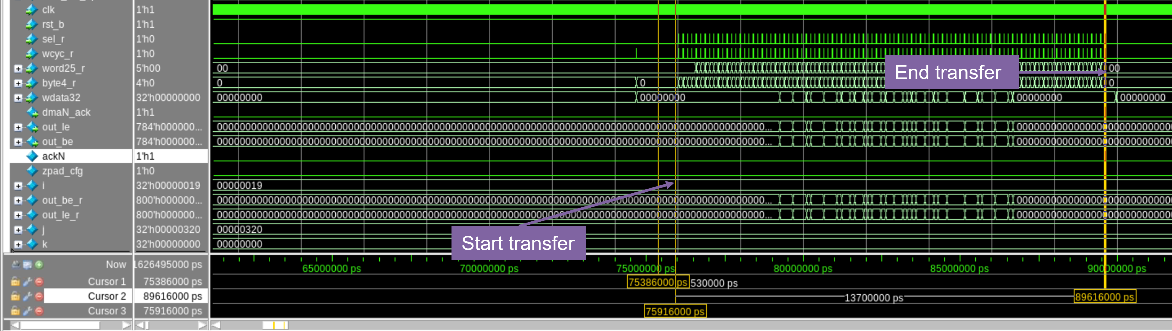
Figure 2. The spike train write transaction from RAM to buffer within SNN IP
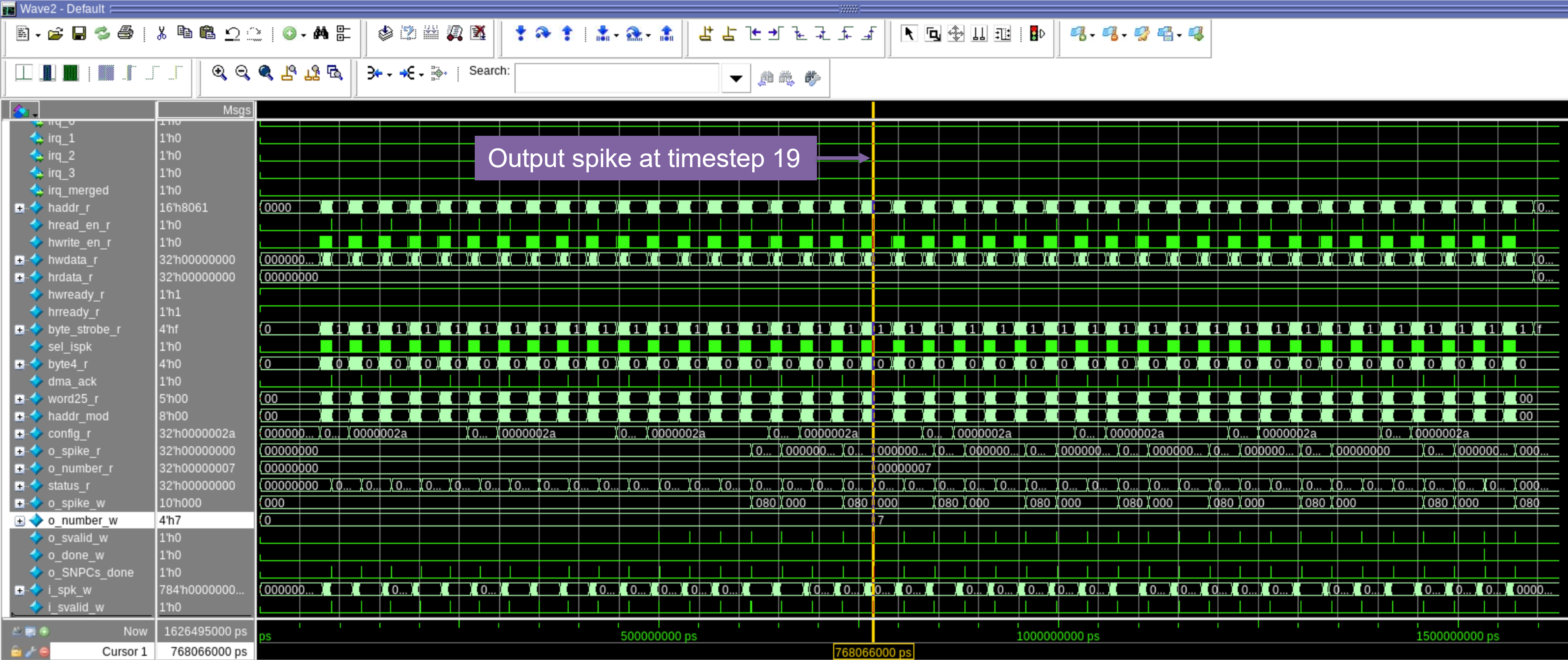
Figure 3. an example result of SNN IP's operation
Team


 Project Creator
 The Anh Nguyen
Research Engineer
at Vietnam National University
Research area: System-on-Chips, Low-power techniques for IoT systems, and Hardware accelerator for Neural networks
Submitted on
Comments
Thanks for the update on the project
Hi,
Happy New Year! Thanks for the update on the project. It would really help us to support you if we could get an update on the milestones as the dates are in the past in 2025. I think it would help us all if we try and work through the next set of milestones for the project and give some estimates of dates for them. No one is going to say these dates are fixed but I always think is a good discipline to have estimates for them.
You can also delete the default milestones that the system added.
Then we can all see a shared plan for the collaboration.
Look forward to hearing from you.
John.
Happy New Year Mr. John and…
Happy New Year Mr. John and members of SoCLabs !
I will review my project and update results that we implemented nanoSoC with our SNN IP successfully on FPGA. Now, we are following ASIC process to synthesis and post-synthesis simulation to analyze our system. I will update next milestones on website soon.
Best regards,
The Anh NGUYEN
Update to Milestones
Thanks for replying. We have made the project tracker in the project page to try and help guide people through their project. I am sorry that the original project just added a set of monthly basic milestones that don't seem to be as helpful as have milestones based on the steps of the design flow.
You can remove the ones that are of no use
Simply click the remove button next to the old and not used milestones.
You have some good and completed milestones and these match workflow stages. There is a entry to have the title be one of the workflow stages. You can simply update them as follows. Select the Edit button next to the Milestone...
Your Milestone 1: Determine scope and focus; this matches the design flow stage "Getting Started".
If you wanted to you could change it as follows. If you start typing getting started, it autocompletes, 'get...' then select it.
One the change has been made then you need to click the update button.
Don't forget to save the whole project page at the end of the edit. You can save it to your drafts until you are happy and then save it to editorial.
I hope this is helpful.
John.
Update to project and Milestones
It would be really good if you could update the project status and the milestones to reflect the work you shared with us in December 2025 and also where you have progressed in the first quarter of 2026.
As you update the milestones it would tidy things up if you remove the old autogenerated milestones and make new ones based on the appropriate workflow stages.
Let us know if you need any help.
John.
Dear SoClabs, I don't see…
Dear SoClabs, I don't see the remove button for deleting the redundant milestones. Please guide me to delete them!
Hi,You should now have the…
Hi,
You should now have the delete buttons. Can you try again?
Thanks,
Richard
Dear Richard, I saw them…
Dear Richard,
I saw them.
Thank you so much,
The Anh
Project tracker
Hi,
Currently the Project Tracker in your project has no items underway or compelte.
Looking at your milestones this does not reflect the good progress you have made. Here is what I see...
Milestone #1: Determine scope and focus
This is like 'Getting Started' in Architectural Design.
Milestone #2: Determine the dataset and SNN model
This is like 'data model' in Architectural Design.
Milestone #3: Determine the requirement IPs
This is like 'IP Selection' in Architectural Design.
Milestone #4: Design SoC architecture
This is like 'Specifying a SoC' in Architectural Design.
Milestone #5: MATLAB simulation
This is fine, the system allows you to have your own named milestones if that is better for you to track things.
Milestone #7: IP verification with cocotb
This is like 'Verification Methodology' in Architectural Design.
If these milestones had their names changes to be milestones from the design flow stages then the tracker would look more like that of Sydney's project.
The good thing about the tracker is you can click on any of the links in the tracker and it allows you to see the design flow stage information and/or update your own milestone.
If you don't need a design flow step then simply uncheck the milestone.
I hope this helps.
John.
Updated Milestone
Great to see the updated Milestones with what has been done. It would be good next to put in some milestones for the work to be done in the future and to plan out the next steps for the project. If you need any help in this please let us know.
John.
Issue with Compiler v.6 when run simulation test_nanosoc
Dear SoC Labs, we are facing an issue when running the project simulation and need support. We are using the accelerator project repository to integrate our IP into NanoSoC. We are using Compiler V6. When I try running the simulation of test_nanosoc with the hello example, the simulation always stops right after generating the trace file tarmac1.log, as shown in the attached image. The full simulation log file is also attached here (run_hello.log).
Could you please give me some suggestions to solve this issue ?
Debugging Support for hello nanosoc test
Hi, sorry, we've only just seen this comment. Its looks like the hex file hasn't been generated during compilation and unfortunately I can't access your log file.
Would you be able to document the steps you've taken before getting to this point so we can get a good idea of whats going on? Have you ran the compilation flow before hand and if so what commands did you run?
Many thanks,
David
Debugging Support for hello nanosoc test
Dear David,
We install the compiler v6, because we don't have the compiler v5. So, after git clone the repository from accelerator-project, I ran "source set_env.sh" to create the environtment. Then, I ran "make clean" in /nanosoc_tech/testcodes folder. Finally, i ran "socsim test_nanosoc TESTNAME=hello" in the top of accelerator-project folder for simple simulation. The simulation progress was hanging as the picture of last comment.
Fix in latest Git repo
Hi,
I think we have now fixed this issue. Essentially bootloader was trying to pull data from uninitialised memory.
If you could pull the latest changes from accelerator-project and try to run this
Daniel
Fix in latest Git repo
Dear Daniel,
Thank you so much for your support. I pulled the latest accelerator project and simulated with DS6 successfully. We will continue to implement our project, and complete it soon.
The-Anh
How are things progressing
I am sorry for the delay in getting in touch. How are things progressing with the project?
I look forward to hearing from you.
John.
Update milestones
Update milestones
Add new comment
To post a comment on this article, please log in to your account. New users can create an account.