SRAM Chiplet
On-chip SRAM in ASICs can use a significant area, which equates to a significant cost. One solution is to make the memory off-chip. This project explores the use of Arm IP to create an SRAM chiplet design. The benefit is that standard memory chiplets can be fabricated at lower cost and used across multiple projects, miminising silicon area to the unique project needs.
Chiplet interface
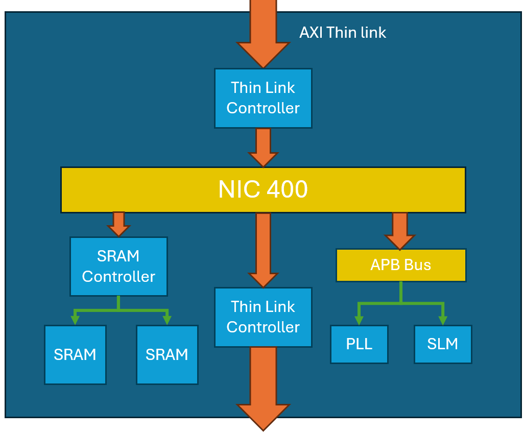
For this project we are using the Arm Thin links (TLX-400) that comes as part of the NIC-450 bundle. The TLX-400 takes a full AXI (3 or 4) or AHB and converts it into an AXI stream interface, it creates a receive interface which takes an AXI stream and converts to a full AXI or AHB interface.
Chiplet Structure
The main thin links interface connects directly to a NIC-400 bus, which has an SRAM controller subordinate (SIE-300), and APB bus subordinate. The SRAM controller connects to multiple banks of high density SRAMs, each bank is 128 KiB in size, with a total of 15 instances to give a maximum of 1.87 MiB.
An APB bus is used to interface with a PLL, which provides the clock for the thin links interface as well as the clock used for the chiplet subsystem. The design also utilises the silicon lifetime monitoring IP that has been provided by Synopsys. The SLM IP allows for monitoring of process, voltage and temperature. Using this IP in conjunction with the PLL, allows measurement of whether the chiplets that are manufactured are typical, slow, or fast silicon to allow adjustment of the PLL frequency depending on how fast the chiplet can actually operate. Ideally a method could be developed for testing dies and their select based on the process corner that they are able to achieve allowing them to be allocated to projects depending on performance needs.
Memory Map
The memory map for this chiplet uses 21 address bits, giving 2MB of total addressable space. The address map is as follows
| Region | Start Address | End Address | Size |
|---|---|---|---|
| SRAM | 0x00 0000 | 0x1F 0000 | 0x1F 0000 (1.9375 MiB) |
| APB Region | 0x1F 0000 | 0x1F FFFF | 0x00 FFFF (64 kiB) |
Testbench
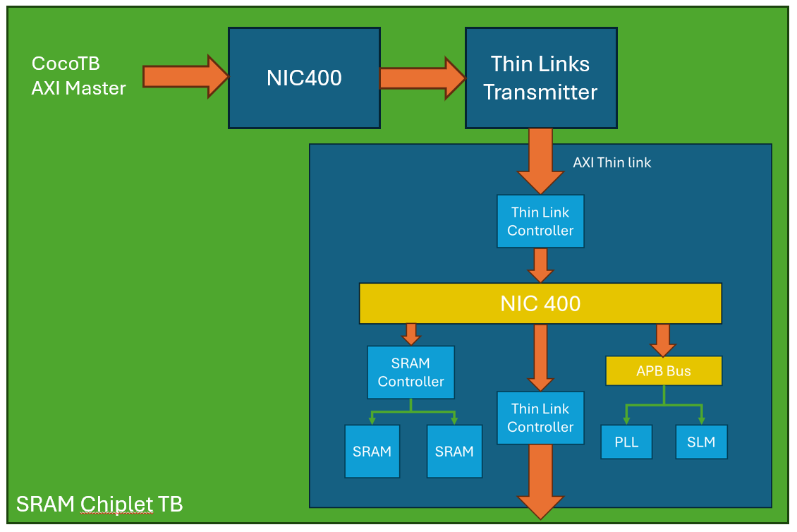
Cocotb will be used as the basis for the test bench, as this can easily generate complex AXI transactions which will make verifying the chiplet subsystem much simpler. The test bench will contain a Thin links transmitter and a NIC-400 bus. This bus just has one manager and one subordinate, and is used to emulate a example system expected from a 'host' chiplet.
Verification Plan
- SRAM Verification
- Write and read to SRAM over thin links of
- Single byte (done)
- 16 bit word (done)
- 32 bit word (done)
- Sequential write and read up to 8192 bytes (done)
- Write and read from bottom and top of address space to SRAM (done)
- Write and read to SRAM over thin links of
- APB subsystem verification
- Read and write to registers
- Read values on reset
- Read voltage, temperature and process values
- Change PLL frequency
Multi-chiplet Testbench
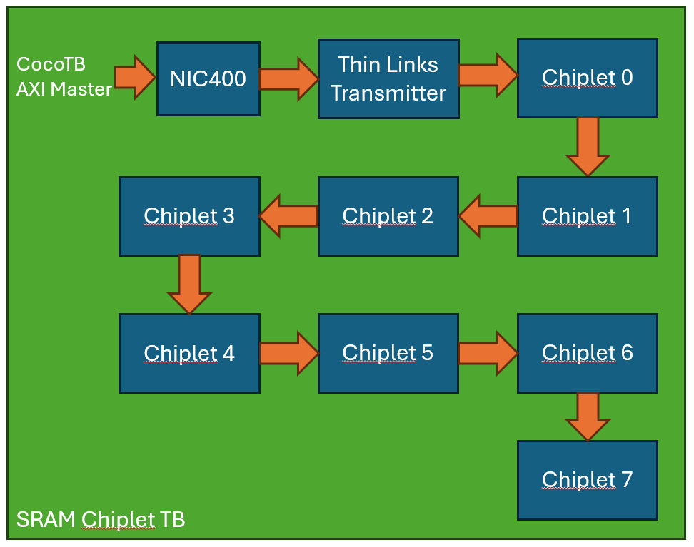
If 2MiB of external SRAM is not enough for the application then it would be useful to be able to connect multiple of these chiplets to a single 'host'. However as the number of wires needed for the thin links interface can be quite high (at least when targeting a mini ASIC area of 1mm2) the architecture decided here is to use a daisy chain structure. Where a read/write request is issued to the first chiplet, and if the address does not correspond to that chiplet, it passes the request along to the next chiplet.
As we also want all of these chiplets to be identical, the way we have achieved altering the address space of each chiplet is to compare a portion of bits in the AWADDR and ARADDR signals to a value set on some of the GPIOs. If these match, then the topmost bits of the AWADDR or ARADDR signal are set to zero (matching the address map above), otherwise AWADDR and ARADDR are left uneffected and passed through the NIC to the outgoing thin links to the next chiplet. In order for this to work correctly, each chiplet much be given an address in accending order away from the host chip (i.e. chip directly connected to the host is given 0, next chiplet is 1, ....) verilog for this is as below:
assign AWADDR_AXI_CHIPLET_IN_i = (AWADDR_AXI_CHIPLET_IN[23:21]==addr_sel[2:0]) ? {11'h000,AWADDR_AXI_CHIPLET_IN[20:0]} : AWADDR_AXI_CHIPLET_IN;
assign ARADDR_AXI_CHIPLET_IN_i = (ARADDR_AXI_CHIPLET_IN[23:21]==addr_sel[2:0]) ? {11'h000,ARADDR_AXI_CHIPLET_IN[20:0]} : ARADDR_AXI_CHIPLET_IN;
Using 3 address select pins allows for up to 8 chiplets to be daisy chained together, for a total of 16MiB.
The concern about daisy chaining these together however raises the question on the bandwidth for accessing the further ends of the chain. However, this actually holds up fairly well, at least for large transfer sizes. For a sequential transfer of 16 bytes you get the following:
| Chiplet Number | Write Bandwidth (Gbps) | Read Bandwidth (Gbps) |
|---|---|---|
| 0 | 4.923 | 5.120 |
| 1 | 3.459 | 3.368 |
| 2 | 2.667 | 2.510 |
| 3 | 2.169 | 2.000 |
| 4 | 1.829 | 1.662 |
| 5 | 1.580 | 1.422 |
| 6 | 1.391 | 1.243 |
| 7 | 1.243 | 1.103 |
Which gives a significant reduction from the first chip to the last chip of 4.6x for reads. However for a sequential transfer of 512 bytes you get the following:
| Chiplet Number | Write Bandwidth (Gbps) | Read Bandwidth (Gbps) |
|---|---|---|
| 0 | 10.291 | 10.317 |
| 1 | 10.015 | 9.990 |
| 2 | 9.752 | 9.683 |
| 3 | 9.503 | 9.394 |
| 4 | 9.267 | 9.122 |
| 5 | 9.042 | 8.866 |
| 6 | 8.828 | 8.623 |
| 7 | 8.623 | 8.393 |
The bandwidth reduction is only a factor of 1.2x when comparing the 0th chiplet to the 7th chiplet. (all of these values are obtained using the same clock frequency for all chiplets of 1 GHz). The reason for this significant difference is due to latency, there are about 7 clock cycles between the AXI transaction being issued by the testbench and being recieved by the NIC in the chiplet. For the 7th chiplet this means a total latency of 56 clock cycles before it recieves the transaction.
If 16 MiB isn't enough for your design, you could either increase the number of addr_sel bits so that you can chain more chiplets together or increase the size of memory on each chiplet to accomodate this. However, at that point it may be worth considering whether a chiplet SRAM approach is really best and whether something like a DDR controller would be much better suited to your application.
ASIC Backend Flow
The backend flow for this chiplet is being developed using Synopsys' fusion compiler, a RTL to GDSII tool.
The constraints for the ASIC implementation are as follows
- Total Silicon area < 2mm2
- Design area < 2.47mm2 as TSMC 28nm design area is shrunk. This equates to 1.57 x 1.57 mm
- On chip clock speed up to 1 GHz
Library compilation
Fusion compiler requires a combined library view to work, which contains both the timing+noise (lib/db) and the physical (lef/gds) views so that it can perform it's placement aware synthesis. So firstly using Synopsys' library compiler, these can be created using the commands below:
create_fusion_lib -dbs $sc9mcpp140z_db_file -lefs [list $cln28ht_lef_file $sc9mcpp140z_lef_file] -technology $cln28ht_tech_file cln28ht
save_fusion_lib cln28ht
This has to be done for all the macros used as well (SRAM, PLL, PVT IP's)
Initial results
So far an initial flow has been developed using 1 process corner (ss 0.81V 125C) and without the IO cells (awaiting on PDK from europractice). below shows the basic floorplan of the chiplet including the macros and power ring + mesh:
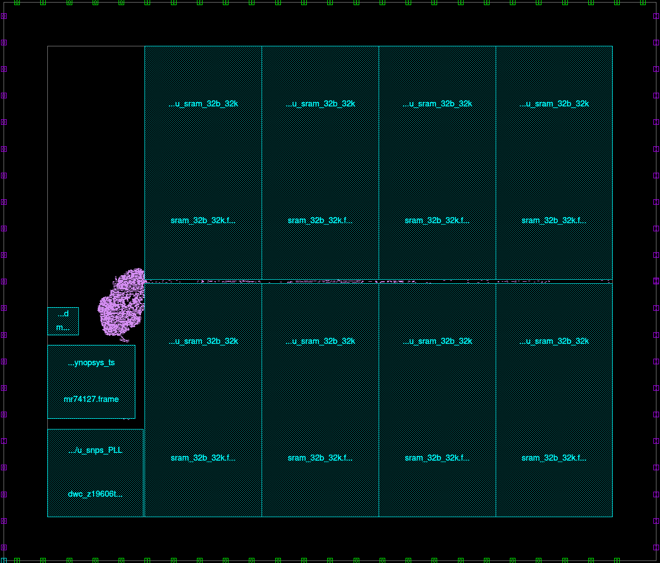
This includes 8x 128KiB SRAM macros using the Arm high density SRAM compiler, for a total of 1 MiB. The total area for this design is 1.79 x 1.53 mm (2.74 mm2) pre-shrink, physical area will be 1.61 x 1.38 mm (2.2 mm2). This is slightly larger than the maximum area we want to have for this tape out, as we want to minimize cost and keep physical area below 2mm2. The area used is also quite wasteful, as the standard cell density is very low (lots of free space unused)
Timing on the single corner closes for a clock of 1 GHz (without any uncertainty). And estimated power usage of this chiplet is 20 mW
Floorplan still needs some exploration as the actual area taken up by logic cells is very small compared to macro sizes, possibly for this same die area another memory macro could be added.
Floor Plan Exploration
The initial floorplanning gave a die size of 2.74 mm2 which is larger than we want. So to decrease the overall area, and make better use of the area, one of the SRAMs has been split into 2 smaller SRAMs. This is slightly less efficient in area, but it means there is more flexibility in the layout.
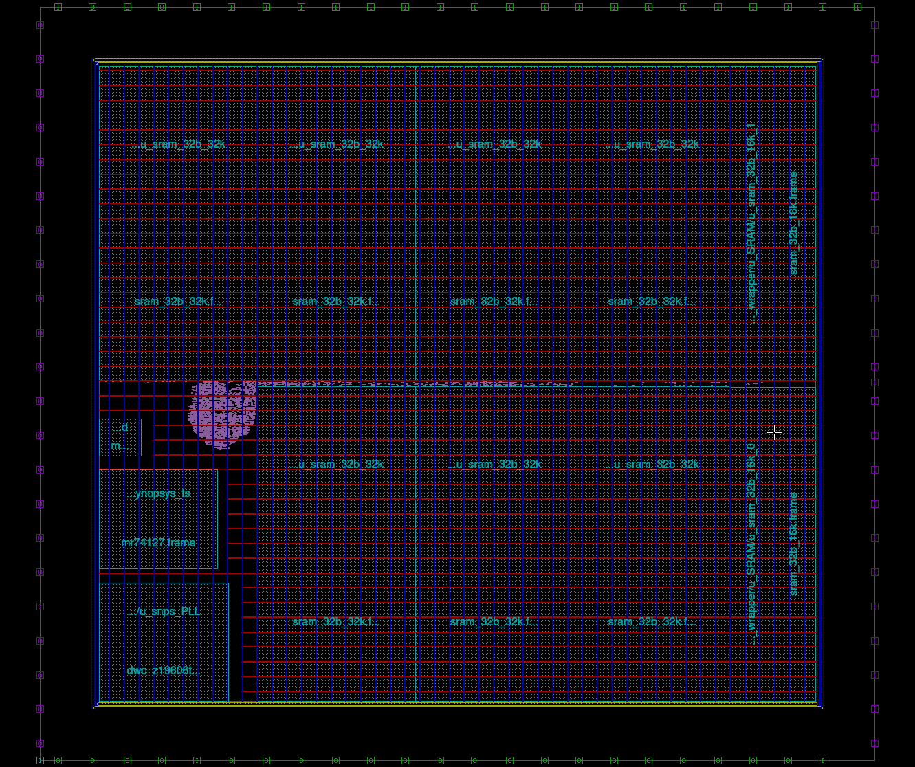
From the above floorplan you can see that much less area is wasted, and the total area now is 1.695 x 1.53mm (2.6 mm2 pre shrink, 2.1 mm2 post shrink). This includes the area for the IO, which currently is unknown (awaiting PDK), so until we are able to place IOs we won't be able to get a final area. So far it has been assumed that the IO cells will be 120 um long.
2MB implementation
After consulting with IMEC/europractice we found that in order to have bumping, we would have to run this on an MPW. Because of this we decided to implement a 2MB chiplet in order to use more area.
Timing closure
So a couple of points came from running through the PnR flow failing in timing.
First was the chiplet interface, this actually was more of an issue with the constraints as I had originally constrained the output connections to the internal clock, when they should be constrained to the clock at the output pin. This was a relatively easy fix and resolved a significant amount of reg2out violations.
Second issue was that the as we have 2 MB of memory, this led to 16x 128KB SRAM instances. The distance between these instances and the memory controller became quite large leading to significant delays. One attempt to fix this was to break up the instances into 4 lots of 4 SRAM instances, giving 4 seperate SRAM controllers. The trade off here is an increase in logic for the extra SRAM controllers and bus logic to these, however there was a significant area of empty space on the design so far, so this wasn't considered a major issue.
Another thin to improve timing was to buffer on both the thinlinks chiplet interface, and on the NIC400 bus to reduce the length of data-paths. After doing these fixes and changing spacing between the SRAMs to reduce congestion, timing has been met for a 1 GHz clock on the chiplet interface and the internal logic (using a 100 MHz reference clock with PLL)
Power network analysis
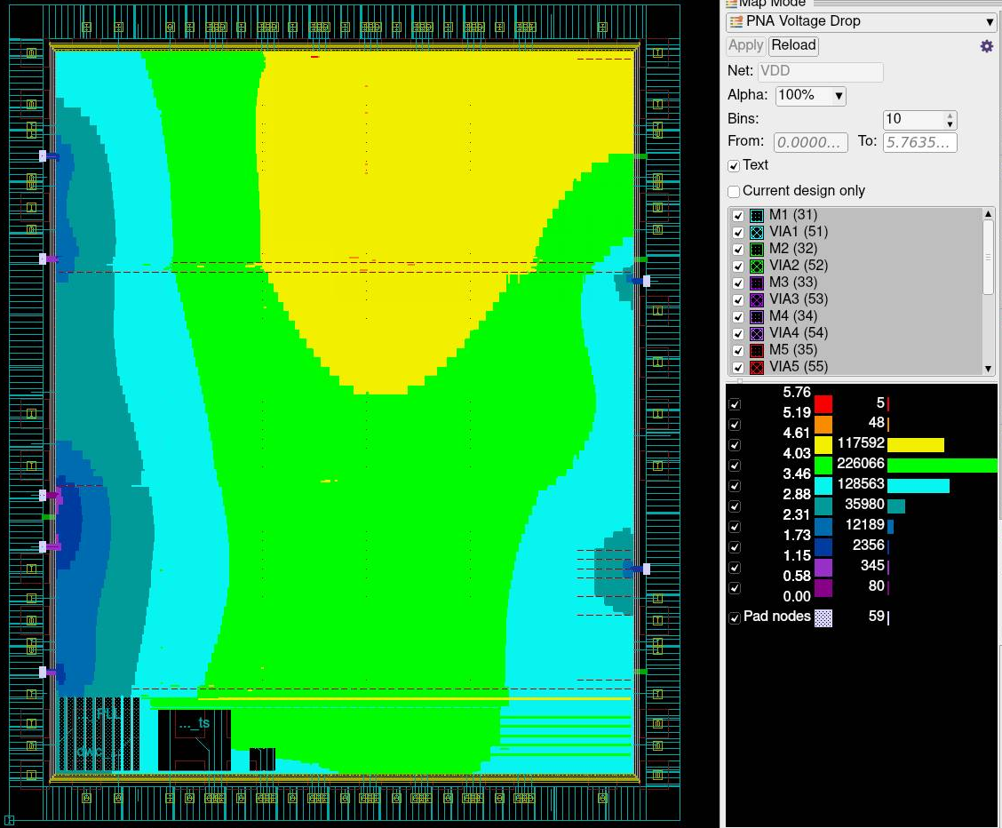
Power network analysis for core VDD shows that the greatest IR drop is 5.74 mV. I think an acceptable value for this design as this is a 0.6% drop
Project Milestones
Do you want to view information on how to complete the work stage ""
or update the work stage for this project?
-
Architectural Design
Design FlowTarget DateCompleted DateDesign the basic architecture and build an initial wrapper for the SRAM chiplet
-
Logical verification
Design FlowTarget DateCompleted DateVerification of the SRAM controller
-
Logical verification
Design FlowTarget DateVerification of the APB subsystem
-
Floor Planning
Design FlowTarget DateCompleted DateBasic backend flow and floorplanning
-
Timing closure
Design FlowTarget DateAim to close design at 1GHz
-
Simulation
Design FlowTarget DateVerify Gate level Sims
Team

Additional Project for:
 Project Creator
 Daniel Newbrook
Digital Design Engineer
at University of Southampton
Research area: IoT Devices
ORCID Profile
 CoreLink NIC-400
 CoreLink NIC-450
Submitted on
Add new comment
To post a comment on this article, please log in to your account. New users can create an account.