nanosoc - baseline Cortex-M0 microcontroller SoC (2024 update)
This second generation (2024 update) of the nanoSoC reference design started development in 2024Q4. It upgrades the initial nanoSoC with additional off-chip communications interface options to better supports both console (STDIN/STDOUT plus ADP ASCII Debug Protocol) and application-dependent 8-bit data I/O streams for improved data transfer on and off chip. The interrupt vectors have been modified to support efficient multiple UART-compatible channel interfaces to support these command and data channels.
Rationale
The nanoSoC reference design provides a baseline microcontroller System on Chip design that supports design, implementation, verification and evaluation of academic developed research hardware such as a custom accelerators or signal processing subsystems. The reference design allows a seamless transition from FPGA to physical silicon implementation that is already silicon proven. nanoSoC also provides a project development environment inclusive of the pre-verified SoC system IP (with diagnostic functionality), software, and validation test benches that may be easily adapted and extended as required.
The design is based upon the Arm Cortex-M System Design Kit, CMSDK, allowing reuse of the AAA pre-verified IP, documentation and software. This has been extended to support simple 'bolting-on' of memory-mapped experimental academic hardware with an appropriate test bench development environment.
The first generation nanoSoC' implemented a bit-serial "FTDI1248" controller for off chip interface to an external host operating on the nanoSoC Test/development Board . This second generation of nanoSoC has an alternative interface to accommodate higher SoC clock frequencies, and support for independent bulk data transfer on- and off-chip to better support data movement through the academic developed research hardware subsystems.
Technical overview
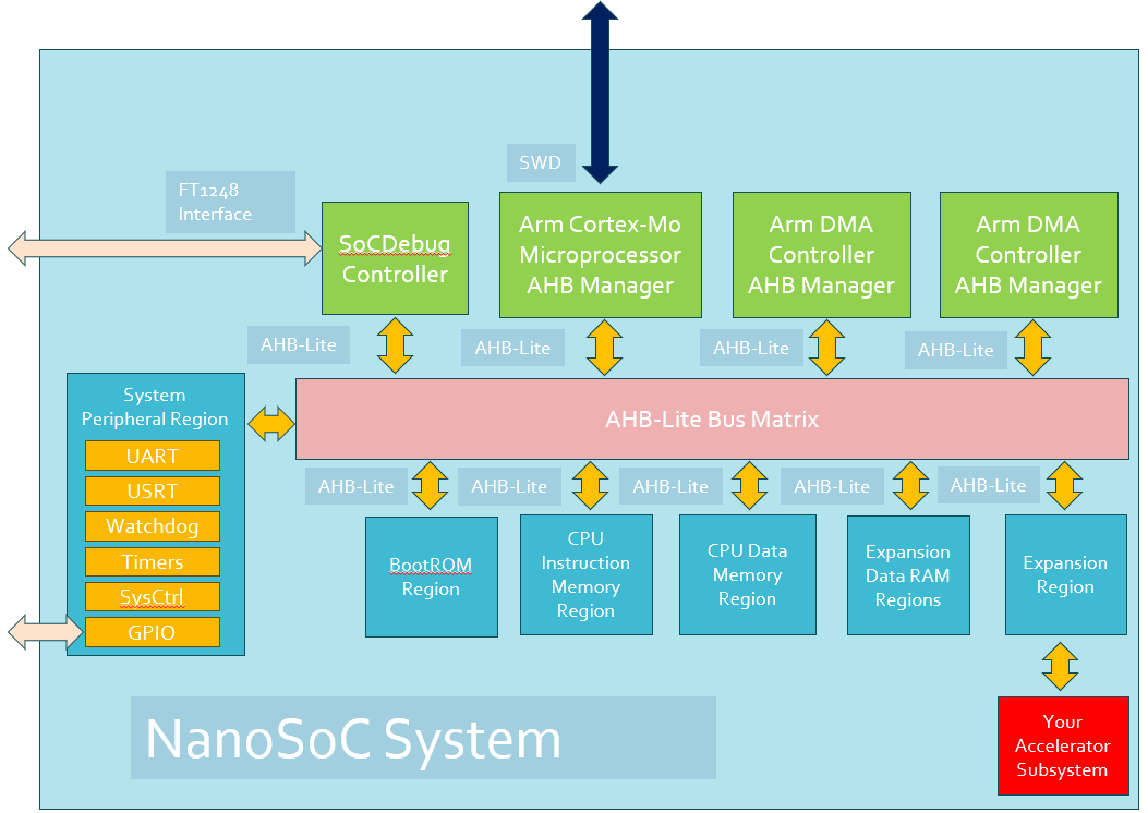
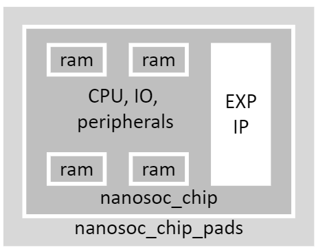
nanoSoC is a Cortex-M0 based microcontroller based SoC design with complete pad-ring support ready for silicon implementation. It has internal address space and control and diagnostic support for integrating custom subsystems or research components:
- CPU - small Arm Cortex-M0 processor with Serial-Wire Debug integrated support
- Boot Monitor - Synthesized ROM bootstrap for MCU
- Code-SRAM bank (configurable size bank of memory primarily for downloaded test programs)
- Data-SRAM bank (configurable size bank of memory primarily for test program data, stack and heap)
- System peripherals (serial communications, General Purpose IO - GPIO, system counter timers and clocks)
- Memory-mapped expansion space
- Optional support for 1 or 2 Direct Memory Address controllers
- Two banks of DMA-accessible SRAM buffer space for concurrent expansion space usage
- ASCII Debug Protocol agent, ADP, with clock independent host interface
Getting started
Soclabs provides an implementation framework to support adding an application-specific hardware accelerator into a SoC based on the nanoSoC microcontroller. The nanoSoC is outlined below but get started quickly you can access the framework resources and review an example hardware accelerator implementation.
Generic accelerator framework
See the git resources and README file for:
https://git.soton.ac.uk/soclabs/accelerator-projectThis instantiates a nanoSoC microcontroller subsystem - that is is provided pre-validated in the the nanosoc_tech sub-respository:
https://git.soton.ac.uk/soclabs/nanosoc_techThe example AES128 hardware accelerator implementation
As a concrete example, a cloned version of the generic Accelerator-Project is extended to add a memory mapped AES encryption engine. nanoSoC supports multiple types of DMA engine to provide efficient data movement for any custom subsytem. This implementation uses an enhanced version of the Arm DMA230 AMBA-AHB Direct Memory Access controller together with test programs written to test both software driven (memcpy) and DMA mapped (dma230) methods.
See the git resources and README documentation at:
https://git.soton.ac.uk/soclabs/aes-128-projectnanosoc Architecture
Interconnect fabric
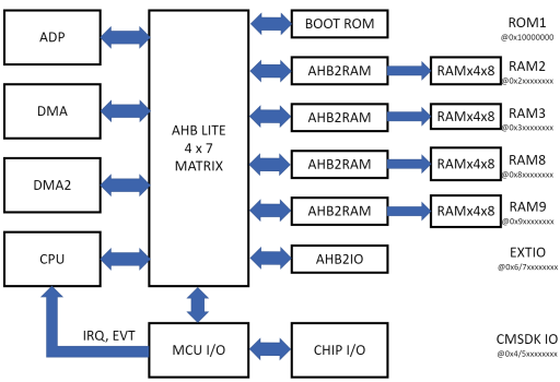
The simple single AMBA AHB bus design of the Arm CMSDK is upgraded in the nanoSoC reference design to a multi-layer AHB-lite matrix that supports up to 4 concurrent access paths to the primary memory and input/output components.
More details of how this bus matrix is generated using the Arm Academic Access tools is described at https://soclabs.org/project/building-system-optimised-amba-interconnect.
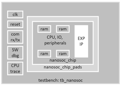
Design and validation testbench
The testbench (tb_nanosoc) provides the functionality to support the provision of:
- system clocking and initialisation
- hardware debug communications port which supports serial communications and ASCII Debug Port agent control and diagnostics
- an Arm Serial Wire Debug controller model for validating software debugger connection and functionality
- an Arm CPU trace model that replicates internal processor state and allows simulated instruction and data trace. This is done for both RTL and gate-level netlist simulation verification to make the verification at each stage of the design process similar, enabling efficient iterations for a design.
FPGA prototyping platform
Two example FPGA example targets for Xilinx(R) Vivado (R) have been provided to date that support hardware prototyping and verification of the nanosoc functionality:
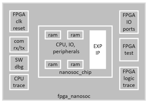
- Xilinx® FPGA platform target with a wrapper layer that provides the mapping from nanosoc chip-level ports (inside the pad-ring) to the FPGA pads as well as providing the target clock and reset control from the board-specific peripherals. This supports board-level evaluation and debug at the desk, usually with a USB-connected JTAG interface.
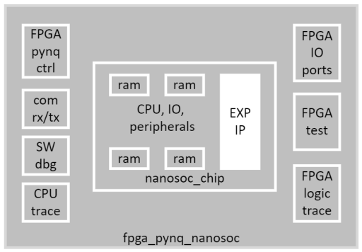
- Xilinx PYNQ® platform target, that supports fully networked validation support and that can be used as a shareable development resource. This uses the integrated Zynq® Arm Cortex-A processor subsystem to provide the linux OS, network stack and python environment with jupyter notebook test code. The target example is the Xilinx ZCU104 evaluation board, that has first-class PYNQ software support.
The baseline FPGA target simply requires programmable logic and memory block resources, and would normally be connected by USB cable direct to the host development system:
The Xilinx Zynq 'PYNQ' platform system development target uses the Programmable Logic (PL) resources to implement the nanosoc design and the Processing System (PS) integrated Zynq-Arm subsystem to provide to run the PYNQ software environment over an Ethernet network connection and allow browser-based SW test and verification remotely from web browser:
Address Map
The address map is kept closely compatible with the Arm CMSDK to allow reuse of the documentation and the example test programs as a staring point. The bus matrix fabric supports additional expansion memory banks and a large uncommitted address mapped region for experimental sub-system interfacing - sufficient to configure, control as well as source and sink workload data to and from memory.
| start-address | end-address | region | notes |
|---|---|---|---|
| 0xF0000000 | 0xF0003FFF | System table ROM | CPU/DBG config |
| 0xA0000000 | 0xDFFFFFFF | Expansion IO space | Experimental IO |
| 0x90000000 | 0x9FFFFFFF | Expansion RAM (hi) | (DMA memory buffers) |
| 0x80000000 | 0x8FFFFFFF | Expansion RAM (lo) | (DMA memory buffers) |
| 0x60000000 | 0x7FFFFFFF | Expansion IO space | Experimental IO |
| 0x40000000 | 0x4FFFFFFF | System IO | (CPU MCU peripherals |
| 0x30000000 | 0x3FFFFFFF | Data memory (RAM) | (CPU heap/stack) |
| 0x20000000 | 0x2FFFFFFF | Code memory (RAM) | (CPU execution memory) |
| 0x10000000 | 0x1FFFFFFF | Bootstrap ROM | synthesized, mapped to 0 |
| 0x00000000 | 0x0FFFFFFF | Vectors, run-time code | Boot ROM -> Code RAM (remapped by boot monitor) |
This address map is fully visible to the CPU software environment and the ADP hardware debug agent.
The optional 1 or 2 DMA controller(s) do not have visibility
For the system IO region:
| start-address | end-address | notes |
|---|---|---|
| 0x40000000 | 0x40000FFF | Timer 0 |
| 0x40001000 | 0x40001FFF | Timer 1 |
| 0x40002000 | 0x40003FFF | Dual Timer |
| 0x40004000 | 0x40004FFF | USRT 0 |
| 0x40005000 | 0x40005FFF | USRT 1 |
| 0x40006000 | 0x40006FFF | UART 2 |
| 0x40008000 | 0x40008FFF | Watchdog Timer |
| 0x4000E000 | 0x4000EFFF | USRT 2 |
| 0x4000F000 | 0x4000FFFF | DMA 0 Base |
| 0x40010000 | 0x40010FFF | GPIO 0 |
| 0x40011000 | 0x40011FFF | GPIO 1 |
| 0x4001F000 | 0x4001FFFF | System Control |
CPU Interrupts
| Interrupt Number | Interrupt Name | Interrupt Source |
|---|---|---|
| 0 | USRTRX0_IRQn | USRT 0 RX interrupt |
| 1 | USRTTX0_IRQn | USRT 0 TX interrupt |
| 2 | USRTRX1_IRQn | USRT 1 RX interrupt |
| 3 | USRTTX1_IRQn | USRT 1 TX interrupt |
| 4 | UARTRX2_IRQn | UART 2 RX interrupt |
| 5 | UARTTX2_IRQn | UART 2 TX interrupt |
| 6 | PORT0_ALL_IRQn | Combined interrupt for any pins on GPIO port 0 |
| 7 | PORT1_ALL_IRQn | Combined interrupt for any pins on GPIO port 1 |
| 8 | TIMER0_IRQn | Timer 0 interrupt |
| 9 | TIMER1_IRQn | Timer 1 interrupt |
| 10 | DUALTIMER_IRQn | Dual timer interrupt |
| 11 | EXP0_IRQn | From accelerator - definable by user |
| 12 | EXP1_IRQn | From accelerator - definable by user |
| 13 | EXP2_IRQn | From accelerator - definable by user |
| 14 | EXP3_IRQn | From accelerator - definable by user |
| 15 | DMA_IRQn | Interrupt from DMA, this is a combined interrupt so can be from any channel |
| 16-31 | PORT0_x_IRQn | I/O pins on Port 0, from pin x, each pin has it's own dedicated interrupt |
Communications channel
nanosoc supports interfacing to an external testbench via an off-chip protocol
See the original nanosoc project (2023; version 1) for the original 4-wire Future Devices "FT1248" serial interface which allowed both FPGA instantiation and implemented hardware at the board-level to a use a standard USB host communication port (Future Devices FT232H chip or similar). Plus an additional two pin Universal Asynchronous Receiver-Transmitter, "UART2" (from the Arm Cortex-M System Design Kit)
As well as a backwards-compatibility mode the communications channel on the new nanoSoC (2024 update) now supports a full dual-ended handshake interface with an off-chip microcontroller or FPGA that implements 4 virtual channels:
| Virtual Channel | Channel | Direction |
| CTX - 8-bit console STDOUT/ADP output | 0 | TX |
| CRX- 8-bit console STDIN /ADP command input | 0 | RX |
| DTX - 8-bit transmit data channel (application dependent) | 1 | TX |
| DRX - 8-bit receive data channel (application dependent) | 1 | RX |
The interface supports 4 AXI-Stream channels and uses a 7-wire packet bus protocol to manage robust data transfer.
DMA230 direct memory access support has been added for the Data TX and RX channels to support efficient block data transfer:
- DTX, enabled by gpio1_dataout[2], generates DMA requests on DMA230 controller channel[2]
- DRX, enabled by gpio1_dataout[3], generates DMA requests on DMA230 controller channel[3]
- (example control programming in nanosoc_system/testcodes/dataio_dma230_tests.c)
The details of the off-chip interface are described in Host-IO | SoC Labs.
The 7-pin interface is mapped onto the seven lower pins of the GPIO Port-1 interface (with Port-1[7] setting the configuration mode):
| Port-1 pin name | EXTIO mode | (FT1248x1 mode) | EXTIO signal description |
| P1[0] | IORQ1_o | (FTMISO_i) | Gray-coded transfer REQuest 1 -> host |
| P1[1] | IORQ2_o | (FTCLK_o) | Gray-coded transfer REQuest 2 -> host |
| P1[2] | IOACK_i | (FTMIOSIO_io) | Transfer ACKnowledge <-- host (async) |
| P1[3] | IODATA0_io | (FTSSN_o) | CRX virtual channel status <-- host (async) / nibble data[0] transfer (sync) |
| P1[4] | IODATA1_io | (UART2RXD_i) | CTX virtual channel status <-- host (async) / nibble data[1] transfer (sync) |
| P1[5] | IODATA2_io | (UART2TXD_o) | DRX virtual channel status <-- host (async) / nibble data[2] transfer (sync) |
| P1[6] | IODATA3_io | (user GPIO) | DTX Virtual channel status <-- host (async) / nibble data[3] transfer (sync) |
| P1[7] | CFG = 0 | (CFG = 1) | Tie low for EXTIO operation |
This provides nanoSoC with 4 robust handshaking byte communications channels.
The Console RX channel is routed to the microcontroller STDIN FIFO, but supports hardware state-machine parsing of input data to support a bare metal physical memory debug assess:
An ASCII 'ESC' (0x1B) escape character is interpreted by the on-chip ADP (ASCII Debug Protocol) agent as the code to enter the ADP hardware monitor mode, signalled by an ASCII ']' character output prompt that then allows the host console to control and debug the SoC address map directly, regardless of whether the CPU is running, and may be used to pre-initialise memory and syetm IO registers and even download code images to run on the CPU. The functionality of the ADP is described more fully at https://soclabs.org/project/hardware-soc-bus-level-debugger
Pinlist
The default pinout found in nanosoc_chip_pads.v is as follows
| Pin/port | Function |
|---|---|
| SE | Scan enable, for use with scan chains |
| CLK | System clock input, currently entire system is driven from this external clock input |
| TEST | Test mode control, if held high during system reset this will enter into scan mode |
| NRST | Active low system reset |
| P0 [15:0] | GPIO port 0 |
| P1 [15:0] | GPIO port 1 (pins[7:0] provide the system-on-chip communications input/output) |
| SWDIO | I/O for serial wire debug |
| SWDCK | Clock for serial wire debug |
Additional implementation wrappers for EuroPractice 65nm tape outs have different pin numbers::
- 44-pin supports bits [7:0] of GPIO ports
- 60-pin supports bits [15:0] of GPIO ports
Team

Reference Design Project for:
 David Flynn
Consultant
at University of Southampton
Research area: Low power system design
 Cortex-M0
 Host-IO
 Corstone 101 for m0/m3
Submitted on
Comments
ARMCC
Hi,
I'm running into problems when simulating the nanosoc. Most tests are passing, but those using debug_tester go into HardFault. It seems it is looking for the stack at address 0x4000E000 which makes no sense to me. Does this test pass on your side ? I'm using cadence xcelium and compiling with armDS6.
Thibaut
Add new comment
To post a comment on this article, please log in to your account. New users can create an account.