Battery Management System-on-chip (BMSoC) for large scale battery energy storage
Battery storage systems are an important source for powering emerging clean energy applications. The Battery Management System (BMS) is a critical component of modern battery storage, essential for efficient system monitoring, reducing run-time failures, prolonging charge-discharge lifecycle, and preventing battery stress or catastrophic situations. The BMS performs functionalities such as data acquisition and monitoring, battery state estimation, cell equalization, and charge protection, making it computationally intensive to manage large scale battery storage. This necessitates the development of a System-on-chip (SoC) solution which can perform real-time and high speed battery management with improved accuracy and efficiency.
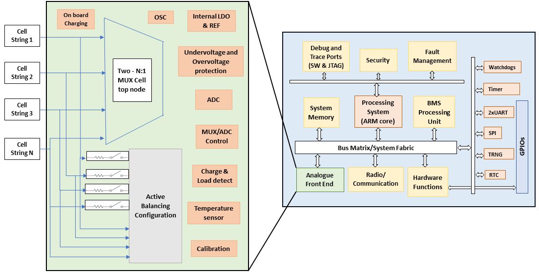
The proposal envisages the development of energy-efficient and lightweight mixed signal Battery Management SoC architecture. The proposed SoC architecture comprises an Analogue front-end (AFE) for voltage, current, and temperature sensing, Analogue to digital converters, a charge protection circuit (overvoltage, undervoltage and overcurrent conditions), a digital signal processing unit, and a master controller with required communication interfaces as shown in the Fig. The AFE architecture also incorporates charge equalization using active cell balancing. Active balancing redistributes charge among cells with imbalanced characteristics as opposed to dissipating energy in the form of heat (as in the case of passive balancing solutions), leading to improved thermal management. The mixed signal SoC offers improved hardware and software components optimization, leading to higher system performance with low latency for data handling and processing.
The SoC architecture can handle multiple cells by integrating low speed sensors with a high speed processor, enhancing the computational capability of edge devices. Additionally, the SoC offers access to cloud resources through the radio transceiver and multiple SoCs can be integrated to form a BMS cluster to provide cloud-based management capabilities. The scalable architecture also promotes ease of integration and reduces the development time for different battery configurations which varies across applications. With modern battery technology evolving rapidly, the SoC provides reconfigurability for adapting to newer technologies without the need to change the underlying processing hardware. The resulting scalable and flexible BMSoC makes it applicable across applications from IoT devices to automotive and renewable energy grid storage.
Functional Specifications of the BMSoC
- Cell Measurement: Upto 16 cells (Rechargeable Li-ion cells)– Combination of 16S1P, 8S2P, and 4S4P (S-series, P-Parallel connection of Energy storage cells)
- Individual cell voltages
- Every parallel string current.
- Accuracy +/-1mV
- Conversion time 37μs/cell (16 bit ADC)
2. Battery monitoring - Digital logic implementation of the Battery State Estimation (State-of-Charge, State-of-Health, State-of-Power) methodology.
- ARM Cortex (M-series) based System-on-chip (SoC) for low power computation.
- Battery Management Acceleration unit (BMS Accelerator) to be interfaced with Cortex M-core for high speed throughput.
3. Cell Balancing: Topology for equalization of charge among healthy and weak cells based on State-of-charge computation for high speed charge balancing (requires string current & individual cell voltage).
- High voltage analog differential MUX.
4. Internal Regulator :-
- 14.4V/28.8V/57.6 , 9A to 12 A current , Ripple 14mV , external switch, Buck boost configuration.
5. Clocking of all subsystems.
6. Charge and Load detection.
7. Temperature sensor integration.
8. OTP (One-time Programmable) Calibration for whole system.
Design Data Inputs:
- Design specifications
- System level modelling and Simulations
- Target CDK - 130/90/65 nm (for high voltage applications)
- Third-Party IPs (Digital and Analog)
Project Milestones
Do you want to view information on how to complete the work stage ""
or update the work stage for this project?
-
Architectural Design
Design FlowTarget DateCompleted Date- Understanding the scope of the competitions and reference designs provided in the soclabs.org
Mixed Signal Design Validation Strategy
Digital Centric mixed signal design flow is chosen for the project
Partitioning of Analog and Digital subsystems
Digital Subsystem - ARM Cortex M3, BMS accelerator, SoC Peripherals, Memory
Analog subsystems - ADC and high voltage MUX, LDO, PWM, High voltage GPIOs.
- Top-level functional block-design for the Analog Mixed-signal (AMS) SoC - completed
-
Logical Design
Design FlowTarget DateCompleted DateDomain Specific Design
Analog Domain
a. Finalizing design specs and schematic design
b. System-level model simulation - completed in Simulink
Digital Domain
a. Implementation of the digital logic using SDK.
b. Software profiling for hardware acceleration.
c. RTL Design of the BMS accelerator - completed
-
Generate RTL
Design FlowTarget DateCompleted Date- RTL design and behavioural simulation of the battery state monitoring methodology.
- Synthesis and FPGA implementation of Hardware software codesign on Zedboard (Zynq-7000 SoC).
-
RTL Verification
Design FlowTarget Date- Generate RTL for ARM Cortex-M3 using Corstone-101 reference design with ETM
- Testing of the reference design peripherals.
- Integration strategy for the BMS accelerator and memories.
-
Behavioural Modelling
Design FlowTarget DateAnalog Design
a. Identifying the PDK for reaching the HV requirement of the sensing front-end part
b. Analog/Mixed signal block design partitioning and Verilog AMS model generation
-
Physical Design
Design FlowTarget DateDigital Design
- Synthesis
- Floor Planning
- Placement and routing
- Functional verification
-
Physical Verification
Design FlowTarget DateAnalog Design
- Analog block IP integration and circuit optimization
- AMS block functional performance verification
- AMS block IP physical import
- AMS block floorplanning
- Analog Physical Design
Digital Design
- Digital block functional performance verification
-
Continuous Integration and Deployment for verification
Target DateAnalog Design
- AMS block IP Layout integration
- AMS block functional post layout validation
-
Physical Integration
Target Date- AMS block physical integration preparation
- AMS block assembly
-
Target Date
-
Target Date
-
Milestone 13
Target Date- AMS block functional block signoff validation
- AMS block preparation for SoC integration
- Dispatch to Foundry for Tape-out
-
Target Date
Team


 Project Creator
 Rashi Dutt
Researcher
at Indian Institute of Technology Hyderabad (IITH)
Research area: Low power VLSI architecture
ORCID Profile
 Processors
 Corstone 101 for m0/m3
![]() Hardware design
Hardware design
![]() Low power design
Low power design
![]() Architectural Design
Architectural Design
![]() Behavioural Design
Behavioural Design
Submitted on
Comments
Physical Integration
Hi,
I am not sure where you are on your project plans but the milestones above had Physical Integration as the target for this month. It would be great to get to know where you have actually got to.
We look forward to hearing from you.
John.
Behavioural Modelling
Hi,
It would be most helpful to get an update on how you are getting on with the Behavioural Modelling milestone for the analog front end and also the progress on the Corstone-101 reference implementation?
We look forward to hearing from you.
RTL Verification Milestone
Hi,
As we are now in July it would be great to get an update on how things are going. Looking at the original milestones on the project there was an RTL Verification milestone at the end of June. How did that go?
We look forward to hearing from you.
John.
Update
Thank you for the update.
Updates to milestones (end of May 2024)
Hi,
It would be good to get an update on your milestones at the end of the month.
You had a Target Date of May 31, 2024 for your Domain Specific Design. How is that progressing?
John.
Hi
Hi
This project is for the…
This project is for the mixed signal Battery Management System-on-chip
An interesting project
Hi,
Thanks for joining. We look forward to collaborating and seeing the project develop. Have you though about the initial Architectural Design milestone? Perhaps you can add an initial idea of how long you feel that will take. It might help to get the project off on the right track. If you have any questions please ask.
John.
Adding a milestone
Adding a milestone is simple. Look at the design flow stages and steps and get a feel for the work. Then select the workflow step as a milestone. Here is an example of the first stage of Architectural Design.
Add new comment
To post a comment on this article, please log in to your account. New users can create an account.