Sensing for Precision Agriculture
Our innovative SoC design for precision agriculture revolutionizes field management by deploying a robust mesh network of sensor-based devices, capable of detailed monitoring and swift response to variations in soil health, erosion, drought, and pest activities. This system not only ensures reliability through its mesh architecture—eliminating single points of failure—but also incorporates diverse sensors for comprehensive data acquisition. It's engineered for energy efficiency to sustain operation throughout an entire crop season, significantly optimizing resource use and reducing waste. By providing continuous and granular data directly from the field, our SoC solution surpasses traditional remote sensing methods like drone mapping, offering enhanced decision-making capabilities and operational cost savings for sustainable agriculture.
GitHub Project: https://github.com/users/lewisMW/projects/1/views/1
GitHub Repository: https://github.com/lewisMW/agriculture-SoC
Project Management
We are a 11-person team. Our main project management tool is GitHub Projects, which is public and viewable here: https://github.com/users/lewisMW/projects/1/views/1.
We have distributed the work into analog and digital teams:
Digital Team Update
Currently the digital team is learning about the ARM M0 processor and the AHB and APB buses and how to create a custom wrapper to interface between the bus and our IP - namely the ADC that the analog team are designing. We have also got Verilator working as a simulator for the DesignStart processor and would be interested to get it working with NanoSoC, (if that's possible). We have 4 members are each currently exploring different ARM IP from the CMSDK.
- Sandin: SRAM IP
- Ben: Slave Mux IP
- Patrick: GPIO Peripheral IP
- Lewis: Timer IP
Aside from the above, Neil is currently looking into FIFO IP to buffer sensor data after being sampled by the ADC and Ted (Kezhi) is investigating a custom wrapper file for the ADC, drawing from https://soclabs.org/project/adc-integration-nanosoc.
Analog Team Update
The analog team have created circuits for different sensor conditioning modules and are currently using QSpice to simulate them with an ADC, which is a free mixed-signal simulator. The 5 members on this team have split up to focus on 2 different sensor types:
- Jaime & Adrian: pH Sensor
- Shin, Erick & Hee: Soil Moisture and Temperature
Currently, both teams have started creating circuits in QSpice to simulate.
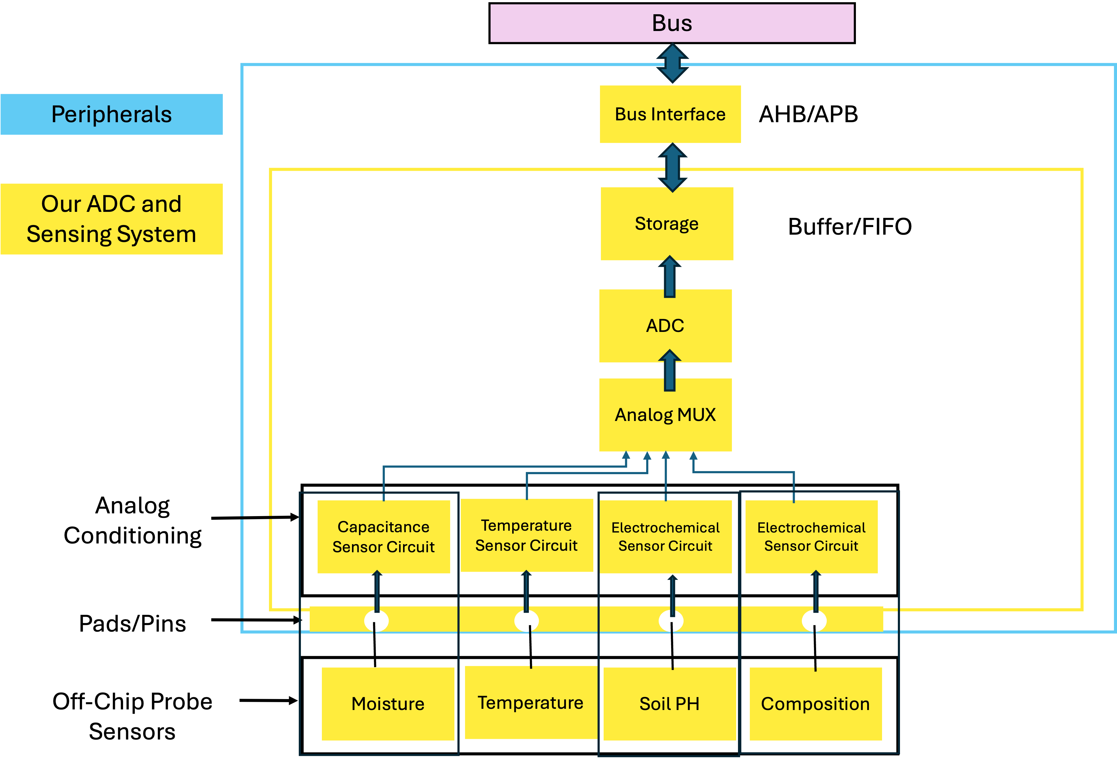
SoC Architecture
The current system architecture is as follows:
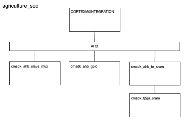
Figure 1: The current system architecture (excluding integration with the AFE).
We have started with a simple system with limited peripherals, restricting our design to the ARM CMSDK IP kit. The motivation behind this is as a learning exercise, such that each team member becomes familiar with the ARM AHB-Lite bus, before moving onto more sophisticated architectures. We plan to migrate to NanoSoC once we get a basic system working (in functional simulation) in Verilator.
Peripherals
- ADC (Analog-to-Digital Converter):Necessary for converting the analog signals from various sensors (such as dielectric soil moisture sensors and electrochemical sensors) into digital data that the processor can handle.
- Real-Time Clock (RTC): Helps in time-stamping the sensor data. depends on which chip we used. (internal or external), Cortex-M0 might not have one inside.
- Timers: We might need Timers as well, it is crucial for managing sensor data collection intervals and controlling the duty cycling of the system, which helps in reducing power consumption.
- Power Management ICs (PMICs): To efficiently manage power distribution and battery charging, especially vital in deploying power-saving techniques like duty cycling.
- GPS Module: For precise geotagging of data, real time positioning for precise watering and management.
- I2C: To consider the cost and low power, we might choose I2C for short connect (interface with RTC, a set of sensors connect over short distances); But we might also need UART for long distances communication.
- Memory Modules : SPI for an SD card - non-volatile memory for data logging.
- Communication (Network) Modules: Depending on the chosen communication protocol (e.g., Zigbee, LoRa, BLE, ZWave, ANT+), for transmitting data across the mesh network.
Memory Mapping
Proposed Memory Map
We connect the peripherals of the SoC to the bus via a bus interface (AHP and APB). Hence, we define the following address map to interface with each peripheral. The ADC of the sensors are fed into a FIFO. Therefore, this FIFO region is responsible for the entire analog frontend of the system.
start-address end-address notes
0x40000000 0x40000FFF Timer
0x40001000 0x40001FFF Real-Time Clock
0x40002000 0x40002FFF PMIC
0x40003000 0x40003FFF GPS
0x40004000 0x40004FFF I2C
0x40005000 0x40005FFF SPI
0x40006000 0x40006FFF SD Card
0x40007000 0x40007FFF LoRa
0x40008000 0x40008FFF FIFO Region
Current Memory Map
Currently, we have the following memory map implemented:
| Start-Address | End-Address | Description |
| 0x40000000 | 0x4000FFFF | SRAM |
| 0x40010000 | 0x40010FFF | GPIO |
You can see that we have started with a very minimal memory map. This was inspired by the HellSoC entry (GitHub) from 2023, as we felt starting from the bottom up would be highly beneficial for our education.
Functional Simulation
We have set up Verilator on our current codebase in the GitHub.
This requires Verilator 5.026, make and gcc and the ARM DesignStart Eval kit. To simulate the system, run make in the agriculture_soc_main directory. To build software to flash the SRAM with, run make in an appropriate software project directory in the software directory.
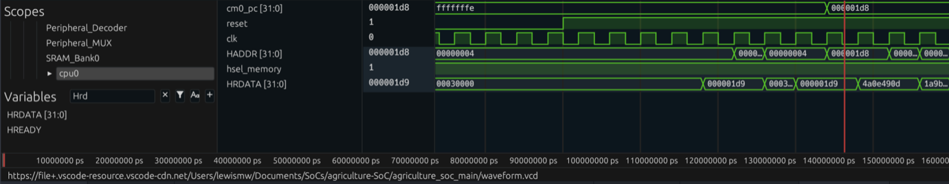
Figure 2: Waveform produced by Verilator for the CPU at startup, viewed in the Surfer waveform viewer.
Analog Front End and Sensors
The architecture of the analog front end is summarised in the following diagram: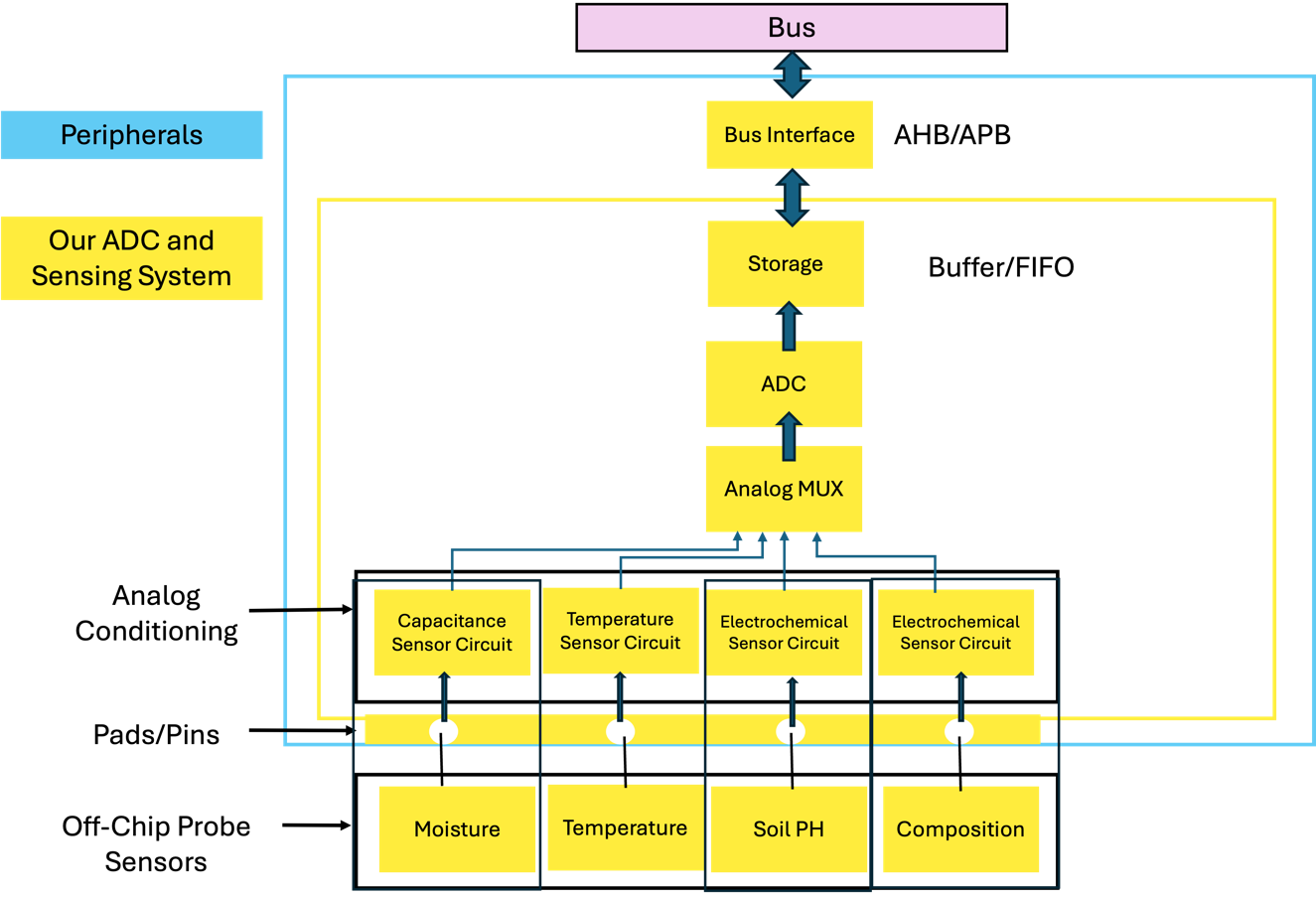
Figure 3: The Analog Front End connected to the AHB-Lite Bus (via APB).
In the above, we have categorised 4 sensing types and are implementing separate signal conditioning / sensor driving modules:
- Moisture Sensor (TDR-based)
- Temperature Sensor
- Soil PH
- Soil Composition
Moisture Sensor (TDR-based)
The standard used in the industry is based on time domain reflectometry (TDR), thus the technology we're implementing is based on TDR. The soil dielectric constant is strongly dependent on the volumetric water content and is almost independent of soil density, texture, salt content, and even temperature [1]. This approach utilized a metal probe of length L in which an electromagnetic wave propagates with a speed that is dependant to the soil moisture content. In [2] an equation for the propagation speed of the wave is presented:
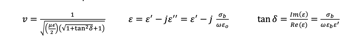
Where:
ε is the complex dielectric permittivity
σb is the bulk electrical conductivity
μ is the magnetic permeability of the soil
⍵ is the angular frequency
εo is the dielectric permittivity of the free space
εb is the bulk dielectric permittivity
If we consider a relatively low electrical conductivity which is the case for homogeneous soil and a high angular frequency, the equation can be reduced to:
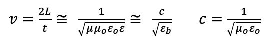
With this expression, we're able to calculate the bulk dielectric permittivity from the time it takes to the electromagnetic wave travel the probe and return, hence 2L.
The proposed diagram for measuring the time is the following
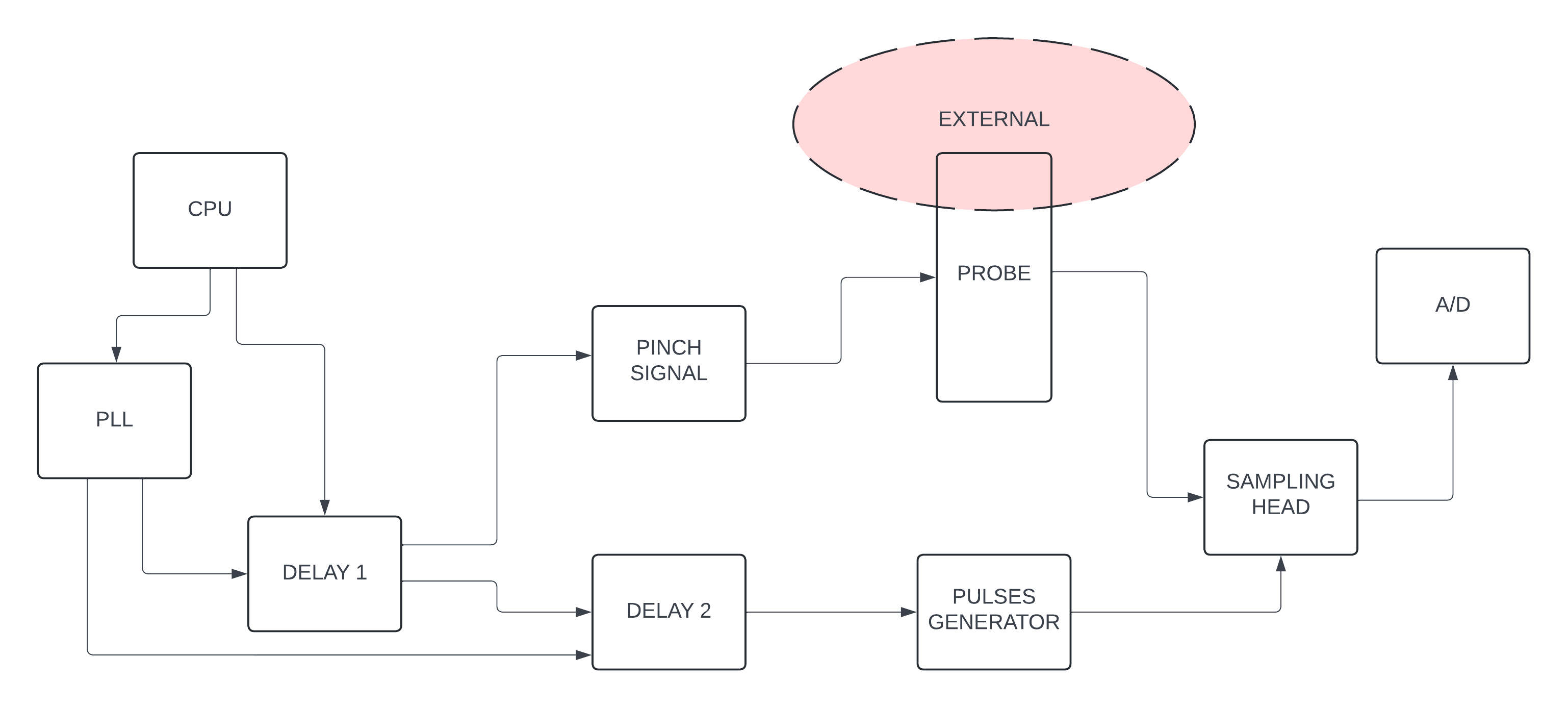
Figure 4: Modules required to implement the AFE for the moisture sensor.
Bibliography
[1] H. Yin, Y. Cao, B. Marelli, X. Zeng, A. J. Mason, C. Cao, Soil Sensors and Plant Wearables for Smart and Precision Agriculture. Adv. Mater. 2021, 33, 2007764. https://doi.org/10.1002/adma.202007764
[2] W. Skierucha, A. Wilczek, A. Szyplowska, C. Swawinski & K. Lamorski. A TDR-Based Soil Moisture Monitoring System with Simultaneous Measurement of Soil Temperature and Electrical Conductivity. Sensors. Poland: Institute of Agrophysics. 2012. https://doi.org/10.3390/s121013545
Temperature Sensor
Temperature sensors can be broadly divided into three categories based on their operating principles:
- Temperature Dependent Resistor Sensor
- Thermistor: A sensor whose resistance changes with temperature, typically available in NTC (Negative Temperature Coefficient) or PTC (Positive Temperature Coefficient) forms.
- RTD (Resistance Temperature Detector): Made using pure metals (usually platinum), these sensors exhibit an increase in resistance as the temperature rises. - PN-Junction Temperature Sensor
Utilizes the PN junction of semiconductors, detecting temperature changes through voltage variations at the junction. Silicon diode temperature sensors are commonly included in this category. - Thermoelectric Sensor
Thermocouple: Measures temperature by detecting the voltage difference at a junction connecting two different metals. If the junction temperatures vary, different voltages are generated, which are used for measurement.
The LM61 is a temperature sensor that utilizes a PN-Junction to detect temperature changes based on variations in semiconductor current with temperature. It can measure temperatures from -55°C to 150°C, and uses a low supply voltage of 3V to measure temperatures from -30°C to 100°C. At temperatures of 0°C and 100°C, the output voltages are 600 mV and 1.6 V, respectively, increasing by 10 mV for every 1°C rise in temperature. The temperature accuracy is within ±2°C.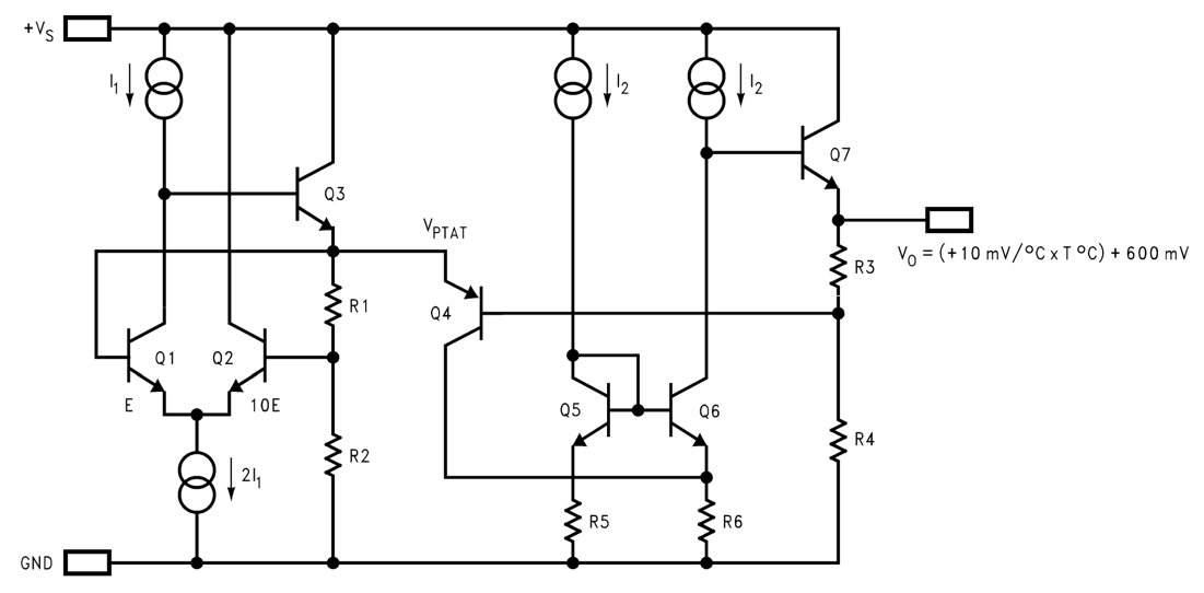
Figure 5: Functional block diagram of the LM61.
Figure 5 presents the block diagram of the LM61, which is composed of seven transistors and several resistors, divided into three main sections: temperature measurement, signal modulation and buffering, and output. Transistors Q1 and Q2 form a pair that acts as a differential amplifier. Q2 is biased by a voltage divider, resulting in an amplification 10 times that of Q1. This difference generates a voltage called V_PTAT (Voltage Proportional to Absolute Temperature), which is proportional to the absolute temperature.![]()
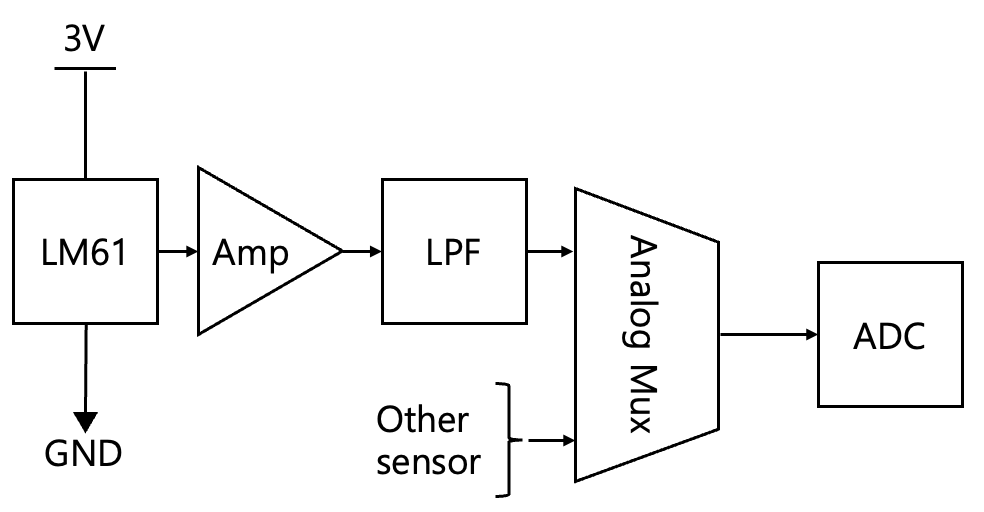
Figure 6: Block diagram of conditioning circuit.
Figure 6 is a conditioning circuit created using an example provided by Texas Instruments. The output from the temperature sensor requires minimal modification and consists of a combination of amplification and filtering.
Soil pH Sensor
Three main categories of sensors have been considered for in situ measurements of soil pH. For the purposes of this competition, which focuses on SoC design, the potentiometric sensor type has been chosen as the focus for our design. This is because it is the most widely used in industry for in situ measurements, and therefore the conditioning circuit we design for this type of sensor will be able to interface with a wide range of products which already exist on the market. It should be noted that the conductometric sensor has been ruled out due to concerns about ion selectivity, but the ion-selective FET (ISFET) sensors may be explored further in later design stages.
A potentiometric pH sensor uses an ion-selective electrode (ISE) pair and measures the potential difference between the reference and the sensing electrodes. The ISE is placed in the soil, and an ion-selective membrane allows H+ ions to pass into and out of the sensing electrolyte. This allows the potential at the sensing electrode to change compared to the reference, depending on the pH of the surrounding soil. The pH of the soil can be inferred from the potential between the electrodes, since voltage can be related to pH via the Nernst equation. A Texas Instruments product has been used as inspiration for the conditioning circuit of the ion-selective electrode, because it addresses key challenges with ISE measurements. These include the dependence of pH/mV sensitivity on temperature, the fact that the ISE produces a bipolar voltage, and the high resistance of the ion-selective membrane. As shown in the diagram, these issues can be respectively combatted by the inclusion of automatic temperature compensation, high input impedance amplification (e.g. voltage follower op-amp configuration) and an offset voltage applied to the reference. A temperature compensation system which incorporates the temperature sensor on our SoC will be designed.
This basic conditioning system has been modelled in Qspice, along with a voltage source to represent the sensor. The model will be refined to include temperature variations, input impedance, temperature compensation, other forms of noise and interfaces with digital components (e.g. for the reference voltage and ADC). A deeper understanding of how each part of the system can be changed to affect key performance metrics (including sensitivity, resolution and accuracy) is needed before the design can be the AFE design can be refined and changed compared to the TI example. Table 1 contains a list of specs taken from existing systems to be used as benchmarks for the performance of our system.
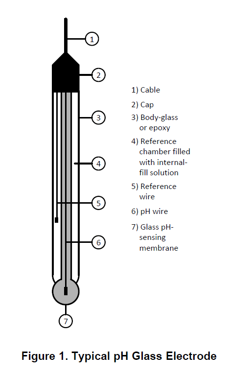
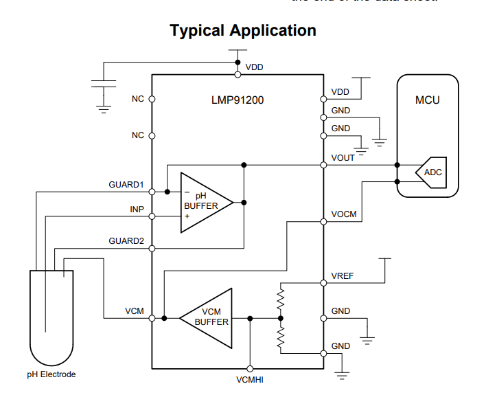
Figure 7: example ion-selective electrode and conditioning circuit, taken from Texas Instruments LMP91200.
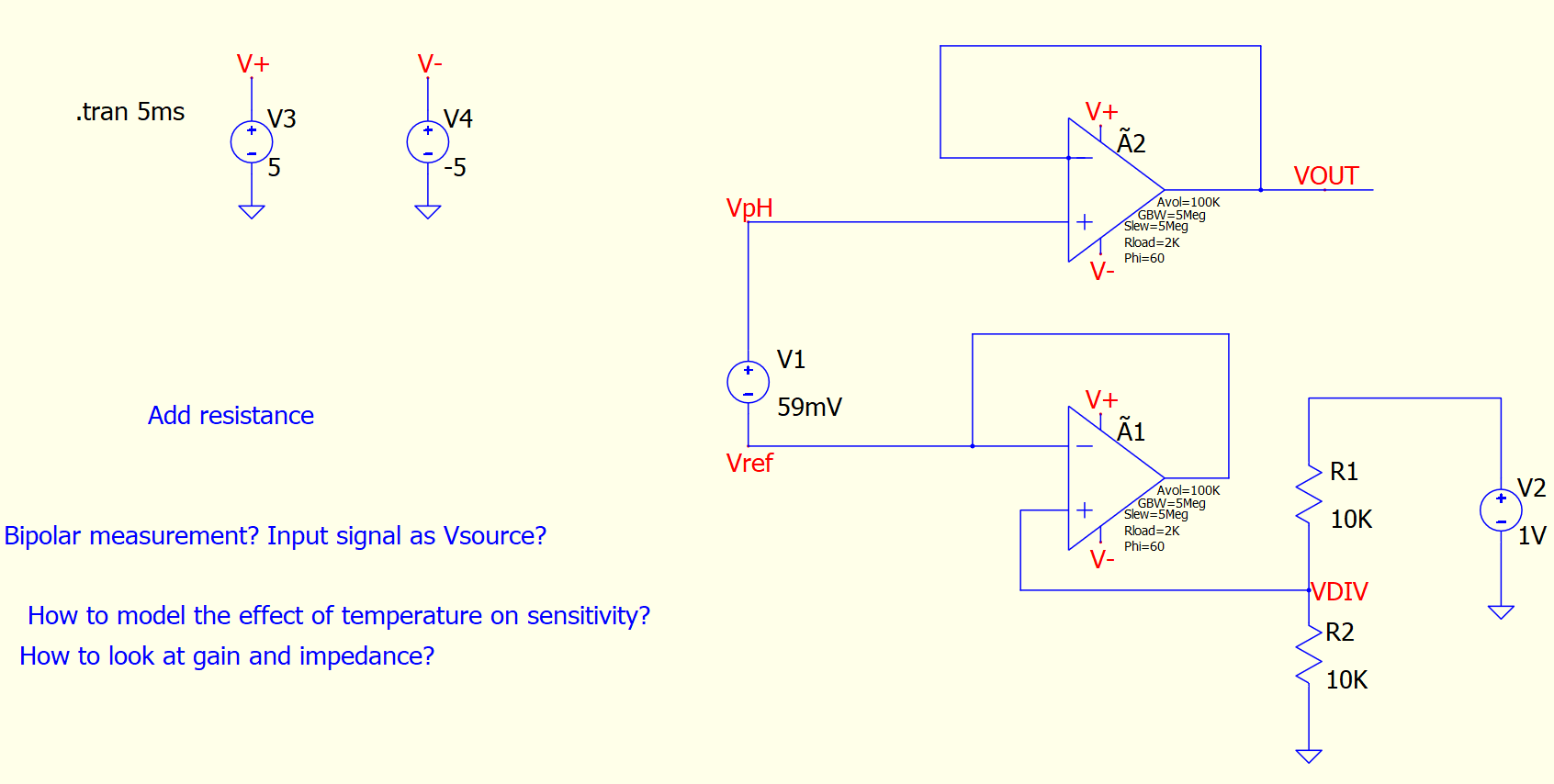
Figure 8: Preliminary Qspice model based on Texas Instruments Application Report available here.
| Specification | Typical Value |
| Range | 2-12 (some achieve 0-14) |
| Sensitivity (mV/pH) | ~60 @ 25 degrees |
| Accuracy | +/- 0.002-0.07 pH |
| Sampling Rate | 800ms |
| Temperature Compensation | Automatic |
| Resolution | 0.01 pH |
Table 1: list of typical performance specifications from a range of pH sensor types (including conductimetric, potentiometric and ISFET).
Bibliography
- Yin, H., et al. "Soil Sensors and Plant Wearables for Smart and Precision Agriculture," in Advanced Materials, vol. 33, no. 20, pp. 2007764, 2021.
- J Bausells, undefined., et al. "Ion-sensitive field-effect transistors fabricated in a commercial CMOS technology," in Sensors and Actuators B: Chemical, vol. 57, no. 1, pp. 56-62, 1999.
- Matthew McCole, undefined., et al. "A low-cost portable system for on-site detection of soil pH and potassium levels using 3D printed sensors," in Results in Engineering, vol. 20, pp. 101564, 2023.
Project Milestones
Do you want to view information on how to complete the work stage ""
or update the work stage for this project?
-
Getting Started
Design FlowTarget DateCompleted DateMilestone #1: Determine project scope and focus.
- Understood competition scope by referring to the NanoSoC design reference and also viewing the 2023 winning entries as examples.
- Voted on the application of precision agriculture as a team.
- Conducted research, including familiarising with existing literature on agricultural SoCs, e.g. https://ieeexplore.ieee.org/document/9789071.
-
Milestone #2: Learning SoC design basics
Target DateCompleted Date- Completing the ARM introductory SoC course Introduction to SoC Design Course - SoC Architecture – Arm®, including resources that are freely available:
- Lectures and Labs: https://github.com/arm-university/Introduction-to-SoC-Design-Education-Kit?tab=readme-ov-file
- Textbook: https://github.com/arm-university/Fundamentals-of-System-on-Chip-Design-on-Arm-Cortex-M-Microcontrollers/tree/main
- For team members with less time, completing the ARM Tutorial on design and prototype of Design Start IP: https://github.com/arm-university/SoC-design-and-prototyping-Research-Enablement-Kit. (We do not have AAA yet).
2. Reviewing NanoSoC:
- NanoSoC Description: https://soclabs.org/project/nanosoc-re-usable-mcu-platform
- NanoSoC Git Repo: https://git.soton.ac.uk/soclabs/nanosoc_tech
- Accelerator w/ NanoSoc Git Repo: https://git.soton.ac.uk/soclabs/accelerator-project
Completed: Team successfully up to date.
-
IP Selection
Design FlowTarget DateCompleted DateMilestone #3: Determine required processor and peripheral features for precision agriculture application.
- Using the NanoSoc processor as a base, identify augmentations like D/A conversion, processing enhancements and power management which tailor our SoC to precision agriculture (soil monitoring) application.
- Identify what constraints these place on the processor, including memory requirements etc.
- Deliverables:
- Draft architectural diagram.
-
Milestone #4: Requirements for mixed signal, communication and processor components.
Target DateCompleted DateMixed Signal
Create list of the required sensors (electrochemical, optical, mechanical, dielectric, temperature) for soil monitoring application and examples of useful sensors available on the market. List all requirements for front-end conditioning of each type of measurement (e.g. precision required, how often each measurement is required and elements of analog circuitry like amplification stages).
Communication (Networking)
- Determine the approach and scope of operation. Discuss and outline the set limits in terms of distance and frequency. Create a sets of block diagram to begin the approach to creating a basic outline. To be discussed with Analog front end team and processor team. Source a minimum of 4 research materials to reference a quick approach.
Update (7/8/24): Listed requirements for electrochemical and temperature. Optical and mechanical have been discontinued due to practicality concerns. Still looking into dielectric sensing and networking.
Update (24/8/24): Networking is on hold for now. Started work on mixed signal sensor components.
-
Specifying a SoC
Design FlowTarget DateCompleted DateMilestone #5: Initial SoC Internal Layout
Using a block diagram (or something similar), to create plan for SoC internal modules, and how these will be connected together. Including modules for the ARM processor core, each sensor, and additional peripherals that may be required (such as memory and networking).
Communication specifications between these modules should also be chosen at this stage (DMA, Bus/Interconnect, FIFO, etc.).
24/8/24: Used ARM DesignStart IP to start with a bare-bones system.
-
Generate RTL
Design FlowTarget DateCompleted DateMilestone #6: APB Wrapper
- Create APB Wrapper for our IP (to interface the Cortex M0 with analog mux, ADC, FIFO queue, etc).
- Document on the SoCLabs page.
- Create unit tests including C code to test APB register access.
Result of WorkWorking NanoSoC + custom peripheral device on Icarus Verilog functional stimulation.
-
Getting Started
Design FlowTarget DateCompleted Date- Investigate and decide on the necessary peripherals such as ADC, RTC, Timers, PMICs, GPS modules, I2C, SPI, and communication modules. Done.
- Define the memory requirements for the SoC and create an address map to interface with each peripheral, ensuring proper allocation and management. Done.
- Move away from the Design Start Kit and migrate to NanoSoC with AAA IP. Done.
- Project Management:
- Get TSMC PDK access through Europractice via S3B (Government). Moved to "Technology Selection" milestone.
- Get Cadence license through existing university contacts. Done.
Result of WorkPDK ongoing NDA issue, to be addressed in a separate milestone "Technology Selection" .
-
Simulation
Design FlowTarget DateCompleted DateSimulation of an integration test of our custom RTL working with NanoSoC.
Completed 5th April 2025.
-
Gain Familiarity with Cadence Workflow
Target DateCompleted DateUsing full Cadence Design Tools workflow for synthesis, implementation, etc. to build up team knowledge of associated processes, in preparation for using this workflow on our RTL..
Result of WorkDeliverable: A word doc guide to the steps required to synthesise and place&route a simple Verilog file.
-
Technology Selection
Design FlowTarget DateCompleted DateAim: Select and obtain a PDK.
- Selected the TSMC 65nm PDK. Done
- Ongoing issues procuring a PDK due to difficulties signing NDAs in our institution.
Fallback: SKY130 open source PDK with Cadence MPW
Result of WorkFell back to the open source option to avoid NDAs.
- SKY130 open source PDK with Cadence MPW.
We hope that there will be an MPW in the future!
-
Behavioural Modelling
Design FlowTarget DateAim: A complete behavioural model of the analog subsystem, with fake sensor input.
Obsolete tasks:
Jupyter Notebook mathematical model of the water moisture sensor. DoneCadence circuit model of the water moisture sensor. Done
Main task: Verilog-AMS model that can be integrated with the NanoSoC:
- Implemented a filter, amplifier, sample and hold module.
-
RTL Verification
Design FlowTarget DateAim: Verify our custom RTL + NanoSoC on an FPGA, with mock ADC input.
Progress: 5x firmware tests simulated on NanoSoC. Found a bug with the RTC.
https://github.com/lewisMW/agriculture-SoC/issues/33
https://github.com/lewisMW/agriculture-SoC/issues/36
-
Design for Test
Design FlowTarget DateAim: Modify our custom RTL with debug counters and to support readout of these.
Progress: N/A
https://github.com/lewisMW/agriculture-SoC/issues/34
-
Preparation
Target Date- Cadence tools setup
- Sky130 Open PDK acquired (Cadence version)
- Todo: decide on SRAM macros
-
Synthesis
Design FlowTarget DateAim: Synthesis the digital component of our design (custom RTL + NanoSoC)
Progress: Synthesised simple Verilog file with Cadence Genus and floorplanned with Innovus using the SKY130 PDK, documented.
https://github.com/lewisMW/agriculture-SoC/issues/35
-
Logical verification
Design FlowTarget DateA collection of manually created tests, derived from those created for the RTL Verification milestone.
This test suite will be applied to the gate level netlist.
-
Floor Planning
Design FlowTarget Date -
Clock Tree Synthesis
Design FlowTarget Date -
Routing
Design FlowTarget Date -
Timing closure
Design FlowTarget Date -
Physical Verification
Design FlowTarget Date -
Tape Out
Design FlowTarget DateTape out for the ChipFoundry September CI2609 https://platform.chipfoundry.io/status?filter=future

Team
 Project Creator
at University of Sydney
ORCID Profile
Submitted on
Comments
Initial layout for SKY130
Hi Lewis,
Just wanted to share this with you. I've been doing some initial work on the nanoSoC SKY130 flow, and above is the layout of nanoSoC. I've not gone through the whole flow yet, but just wanted to reassure you that we should have plenty of space. The 4 blocks there are the SRAMs, the grey bits in between are all the standard cells (highlighted green is the bootrom)
We've not got a bootrom macro (as OpenRam doesn't seem to generate timing views for this), but we should be fine just hard coding this with tie cells
Still work to do on timing and everything but hopefully this gives a bit of a picture
Daniel
Project review meeting update
Hi,
A really useful project update today. It was great to here Daniel Newbrook talk about the SKY130 PDK and the actual I/O planning for the pads, etc. Adding analog to a nanoSoC design that can be sensitive to noise means care needs to be taken in the I/O design and also the power delivery to parts of the design. To keep nanoSoC design small stable power supplies are delivered from off chip via the ASIC test board. There was a discussion on the use of LDO regulators but with many other design challenges to address a simple but practical approach is needed. Separate off chip power supplies to manage noise would seem a reasonable approach.
Looking into the detail of the pad ring Daniel gave an overview of the responsibilities this area of design covers that many digital only designers often do not have insight of. The pad frame covers things such as ESD protection as well as other fabrication considerations. There was a discussion on the pad circuitry and the difference between the standard digital GPIO pins and analog circuit pins. Daniel had been looking into the SKY130 library in this area at the GPI bypass which allows a standard GPIO pad to become an analog pad.
There was also a discussion on using a default pad ring design or whether placing specific I/O pad macros would benefit the project. It really felt like we were starting to get the back end Physical Design flows initiated and as we move into June is going to be an interesting time for the project.
John.
Updated Milestones
Thanks for the updated Milestones.
John.
Milestone #6: Migration to NanoSoC
Luis,
Now you are back home it would be good to get an update on the current milestone. Do we need to set up a call on the ADC?
John.
Milestones
David Mapstone (right) and I (left) were pleased to host a visit of Lewis (centre) to Southampton on a rather cold January day, bet he is happy to be back in Sydney for the weather! Great to catch up on the project and thanks for updating the milestones.
Despite attempts to make the paperwork easier for Universities it seems we have more to do in 2026 to enable students to take part. I will enjoy working on that.
Thanks for the updated milestones. We look forward to the next Teams call and moving forward on them.
Could you expand on Gain Familiarity with Cadence Workflow: word doc guide to the steps required to synthesise and place&route a simple Verilog file.
Is this something the broader SoC Labs community could benefit from and can you let us know what we should do better to describe the cadence flow in our 'design flow' pages?
Updates to milestones (end of July 2024)
It would be great to get an update on where you have got to with this project.
We look forward to hearing from you.
Reviewing NanoSoC
Hi,
As you go through your work of Reviewing NanoSoC we would welcome any feedback both positive and things you would like improved and of course any questions you have.
We look forward to hearing from you.
John.
Hi John,We have just got AAA…
Hi John,
We have just got AAA finally, so we can properly go through it!
All the best,
Lewis
Project structure with AAA and nanoSoC
I think you have been working up to now using the Design Start version of the arm IP. I have seen some comments about looking at the HellFire SoC implementation as that also used the Design Start version of the M0 CPU. Hopefully, now that you have AAA access, you can utilise the full AAA arm IP within a Project structure such as the one we have made available with nanoSoC. If you need any help with this please do let us know.
NanoSoc
Yes, we have been able to get Verilator working with the Design Start IP - this has been a good educational exercise for the team.
We will look into setting up NanoSoC now that we have access to ARM IP.
Updates to milestones (end of May 2024)
Hi,
It would be good to get an update on your milestones at the end of the month.
I think you edited Milestone #1 to be'Determine project scope and focus'
How is that progressing?
We look forward to hearing from you.
John.
Initial Milestones
Thanks for adding these. They look good.
You can keep adding milestones as you go. Don't forget to submit the changes. Change from Drafts to Editorial and press Save .
If you edit your project and go to the bottom you will see;
Latest Milestones
Hi,
Thanks for the latest milestones they really help share your plans for the SoC development. Let us know if you need any support and help. We look forward to hearing more as you develop your plans for the specific sensors.
John.
Any update on the sensor side?
While you have been waiting for AAA have you made any progress on the sensors side?
Actually, was pasting it in…
Actually, was pasting it in when you commented!
Add new comment
To post a comment on this article, please log in to your account. New users can create an account.