ADC Integration in nanoSoC
Rationale
The aim of this project is to define a mixed signal subsystem for the nanosoc reference design.
The mixed signal subsystem should be able to sample analog signals at a regular sampling rate, and transmit a digital representation of this signal to the rest of the nanosoc system. In order to interface with real-world signals in a digital System on Chip ("SoC"), an analog to digital conversion ("ADC") is needed.
Technical overview
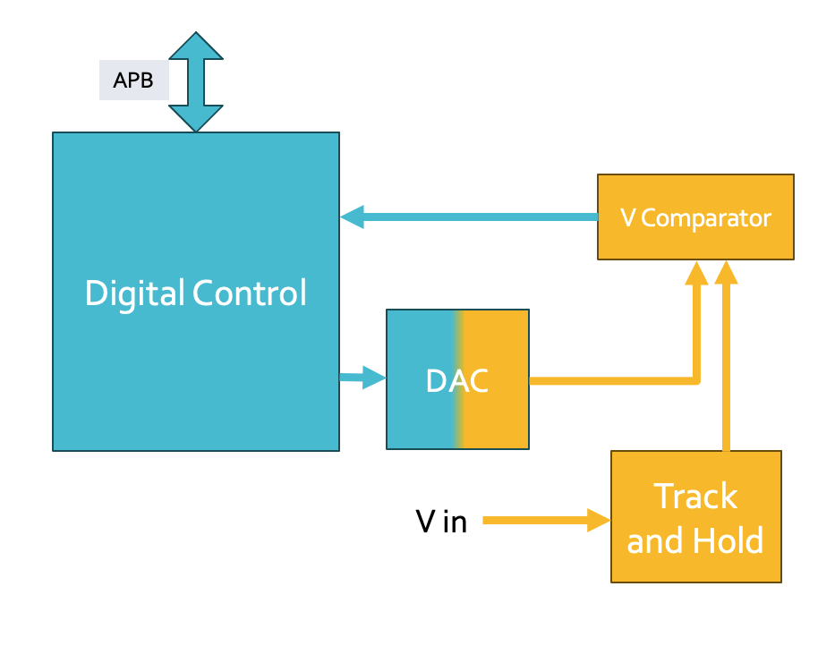
From the digital side, there needs to be an interface for the system that can be used to read and write to registers within the ADC, these include data as well as some control registers. On the analog side there needs to be a way of sampling the analog signal and converting it to a digital representation.
Analog to digital conversion
For this project the analog to digital converter portion of the subsystem has been chosen to be a successive approximation register ("SAR") type ADC. These type of ADCs are common in microcontroller SoCs which is in line with the design target for nanoSoC. They provide a good, power efficient ADCs for reasonable speed, accuracy (common use ranges from 8 to 16 bit resolution) and implementation area.
These type of ADC work by comparing the input signal, which is held on a Track and Hold to a signal produced by a digital to analog converter ("DAC"). This DAC is fed digital values by the ADC control logic which represent an estimate of the voltage. Each estimate is viewed by the Comparitor as above or below the input signal and feedback to the controller which adjusts the estimate until the system converges when the two match and the digital value is stored in the output register. In nanoSoC that is available for transmission on the Advance Peripheral Bus ("APB").
Specifications
For nanoSoC these are the target specifications that have been determined for the ADC:
- 8 bit resolution, this is a reasonable trade of between accuracy, speed of convergence, area and power.
- 100 kHz sampling rate, due to the design an SAR ADCs power dissipation scales with the sample rate.
- 0-1.2V conversion
- Low differential nonlinearity and integral nonlinearity. In general the linearity of the overall ADC is limited by the linearity of the DAC.
- Low power (<1mW)
FPGA prototyping
To be added
Architecture
Digital to Analog Convertor
For simplicity, the DAC design is based on a R-2R summing amplifier. For a more detailed explanation of how this circuit works, you can find a good resource here.
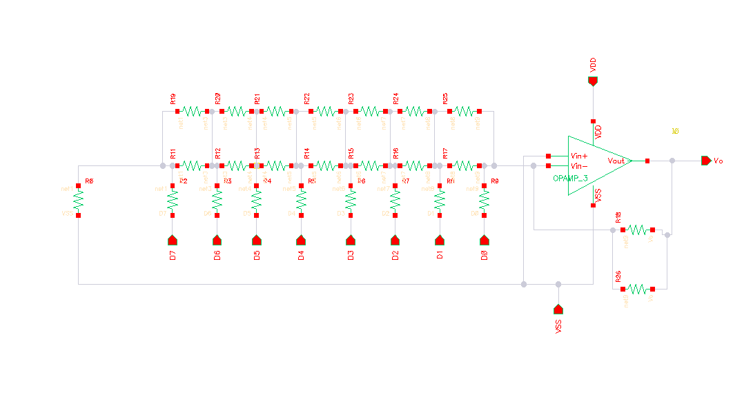
The schematic above shows the implemented R-2R DAC subsystem. Due to the sizing restrictions of the resistors in the TSMC65nm PDK, in order to get the correct resistor values, parallel resistors are used for the R values, with each resistor having a value of 2R (the actual value is 335 Ohm).
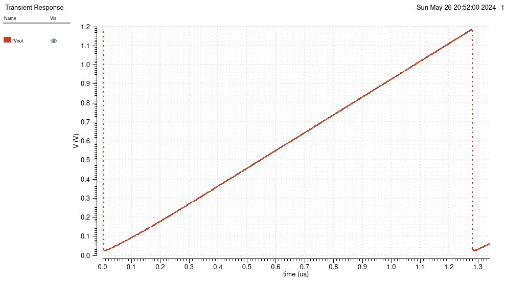
The Operational Amplifier ("opamp") design is the same one used in the TSMC 65nm PLL. As the gain of this opamp setup is 1, the available bandwidth of this should be around 240 MHz. This is consistent with the simulations of the DAC, as the settling time for the conversion of the MSB is around 4ns. An SAR ADC's speed is limited by the settling time of the DAC. This suggests that this DAC circuit will work well for an ADC sampling frequency of 100 kHz.
Simulating the DAC with increasing binary input shows a fairly linear increase in voltage from ~0V to ~1.2V. By simulating the change in voltage 1 bit at a time, the actual voltage for each bit can be measured. The results from this are shown below for each bit from MSB to LSB. The integral nonlinearity is -8.14 LSBs, this is the sum of all differences in number of LSBs.
| Ideal Voltage (mV) | Actual Voltage (mV) | Difference (mV) | Difference (LSBs) |
|---|---|---|---|
| 600.00 | 590.22 | -9.78 | -2.09 |
| 300.00 | 291.78 | -8.22 | -1.75 |
| 150.00 | 142.33 | -7.67 | -1.64 |
| 75.00 | 69.09 | -5.91 | -1.26 |
| 37.50 | 34.07 | -3.43 | -0.73 |
| 18.75 | 16.94 | -1.81 | -0.39 |
| 9.38 | 8.47 | -0.91 | -0.19 |
| 4.69 | 4.29 | -0.40 | -0.09 |
Digital Interface
For the digital interface:
- APB read and write
- Clock divider control
- Enable/disable ADC (with clock gating), to enable power saving where the data acquisition is not continuous or to isolate measurements.
- Busy status register
- Interrupt enable
Interconnect fabric
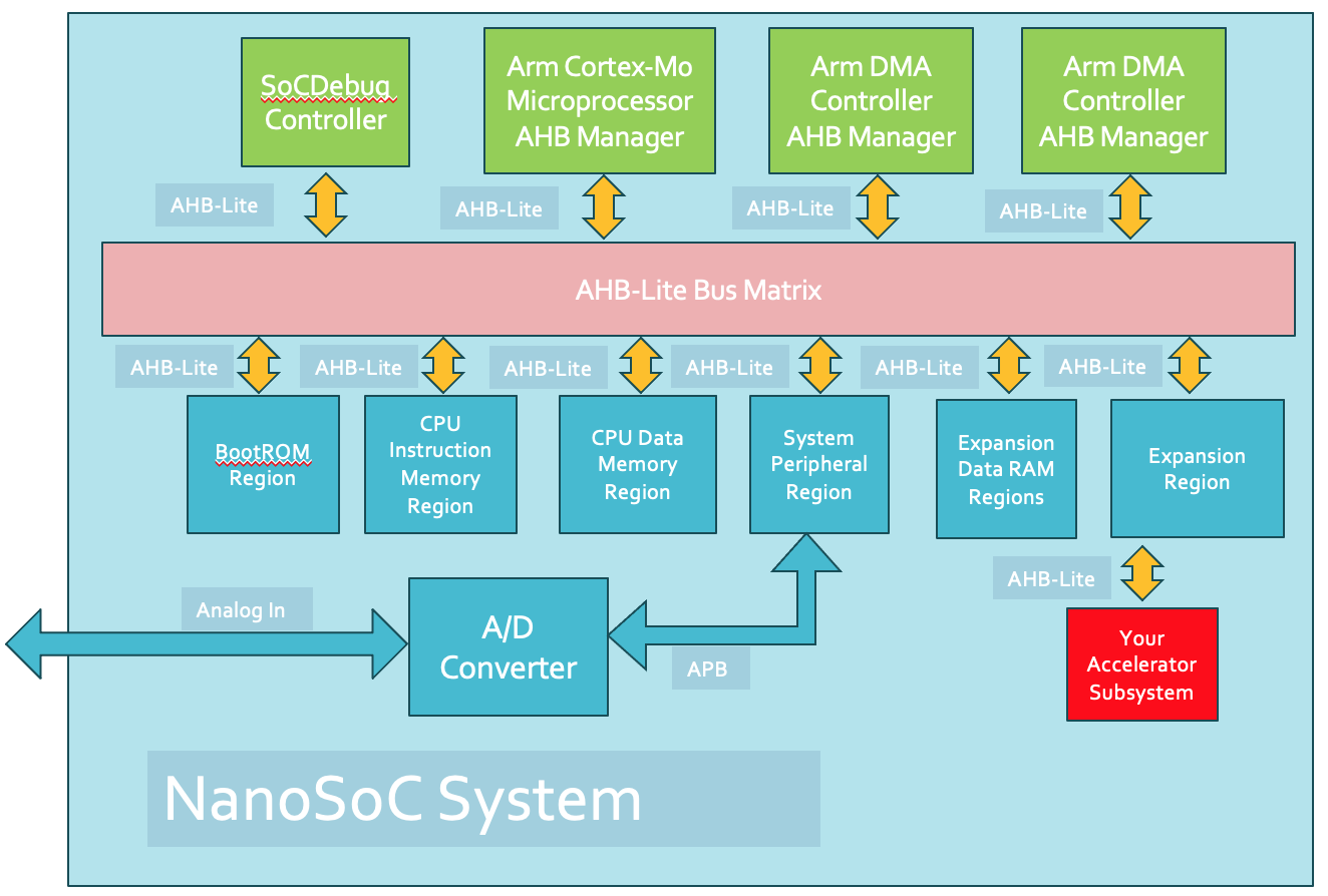
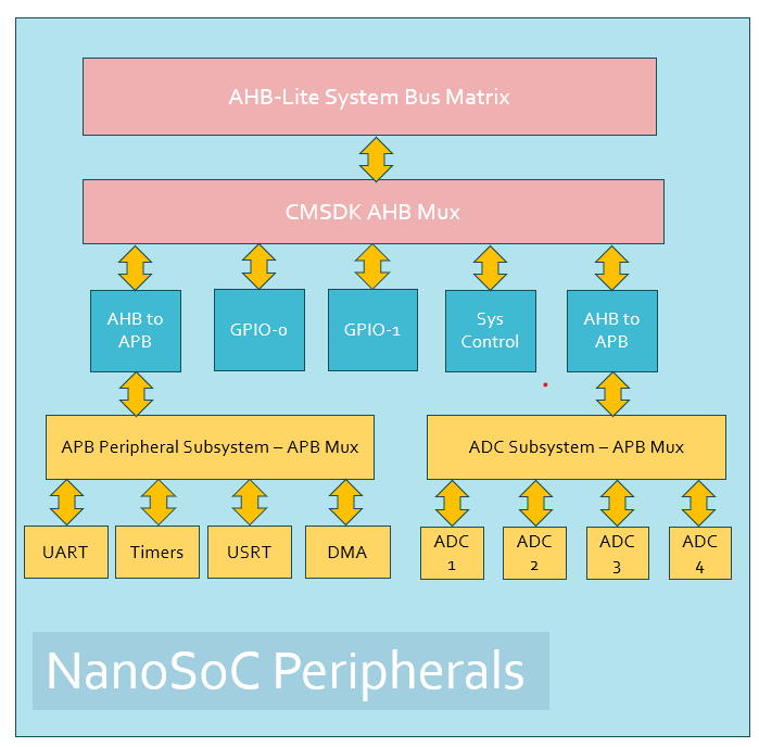
The nanosoc reference design bus matrix is generated using the Arm Academic Access tools as described in Building system-optimised AMBA interconnect. The bus system within the SoC should be carefully planned to manage bandwidth and access latency. The nanosoc design uses a Multi-layer interconnect that allows multiple bus transaction Initiators (traditionally called 'Masters') to communicate concurrently with the particular memory-mapped target responder peripherals or subsystems (traditionally called 'Slaves')
The Advanced Peripheral Bus ("APB") is not pipelined and is used to connect to low bandwidth peripherals and is optimized for low power consumption and reduced interface complexity. An AHB-APB bridge acts as a responder on the nanosoc AHB bus synchronizing the time domains of the high-speed AHB bus with the lower-speed clocks used by peripherals.
This project will utilise the simple APB bus interface for integration of real-world analog signals into nanosoc. In order to add this to the nanosoc peripheral region, an extra port has been added to the AHB MUX, to include a AHB to APB bridge and APB Mux for multiple ADC's to be added in the system. We end up with a subsystem as shown below for the ADC integration in nanosoc
Address Map
The address for a peripheral is determined by the bus to which the peripheral is attached. nanosoc has a defined address map with the range allocated to the System Peripheral Region. We are going to add an ADC region at the end of the nanosoc peripheral bus region as shown below
| start-address | end-address | notes |
|---|---|---|
| 0x40000000 | 0x40000FFF | Timer 0 |
| 0x40001000 | 0x40001FFF | Timer 1 |
| 0x40002000 | 0x40003FFF | Dual Timer |
| 0x40004000 | 0x40004FFF | UART 0 |
| 0x40005000 | 0x40005FFF | UART 1 |
| 0x40006000 | 0x40006FFF | UART 2 |
| 0x40008000 | 0x40008FFF | Watchdog Timer |
| 0x4000E000 | 0x4000EFFF | USRT 2 |
| 0x4000F000 | 0x4000FFFF | DMA 0 Base |
| 0x40010000 | 0x40010FFF | GPIO 0 |
| 0x40011000 | 0x40011FFF | GPIO 1 |
| 0x4001F000 | 0x4001FFFF | System Control |
| 0x4002000 | 0x4002FFF | ADC Region |
CPU Interrupts
Define the system interrupt for a measurement.
Integration Modelling
To develop the integration of an ADC in nanosoc, a simplified verilog-AMS model of an ADC was used. Verilog-AMS allows for the simulation of analog and mixed signal modules alongside digital verilog or other HDL's. The benefit of using verilog-AMS is that it is also technology independent so can be simulated without needing access to PDK's, the disadvantage is that it is not synthesizable, however the analog/mixed signal modules can easily be replaced with macro's of the final IP's.
The development of the ADC subsystem was done within the nanosoc test environment. The benefit of this is that it was easy to develop and run C code from the Cortex-M0, without the need for creating a testbench that could handle APB transfers.
APB Register interface behavioural modelling
The APB register interface is handled by a simple state machine. This FSM waits in the APB_IDLE state until the PSEL signal goes high, and checks whether PWRITE is asserted or not. If PWRITE is high it will go into the APB_WRITE state, otherwise the APB_READ state. Within these states it either writes to or reads from the register as pointed to by PADDR. You can see in APB_WRITE that PSLVERR is asserted if certain read only registers are attempted to be written to. And currently the only registers that are R/W are the clock divider (CLK_DIV) and ENABLE (which enables the ADC if bit 0 is written as 1).
PREADY is asserted high if the state machine is in either APB_READ or APB_WRITE, otherwise it is 0.
// APB interface
localparam  APB_IDLE = 2'd0,
            APB_WRITE = 2'd1,
            APB_READ = 2'd2;

reg [1:0] apb_current_state;
reg [1:0] apb_next_state;

always @(posedge PCLK or negedge PRESETn) begin
    if(~PRESETn) begin
        apb_current_state <= APB_IDLE;
        PSLVERR_reg <= 1'b0;
    end else begin
        apb_current_state <= apb_next_state;
    end
end

always @(*) begin
    case(apb_current_state)
        APB_IDLE: begin
            PSLVERR_reg = 1'b0;
            if(PSEL) begin
                if(PWRITE) begin
                    apb_next_state = APB_WRITE;
                end else begin
                    apb_next_state = APB_READ;
                end
            end
            else begin
                apb_next_state = APB_IDLE;
            end
        end
        APB_WRITE: begin
            case(PADDR)
                10'h000: PSLVERR_reg = 1'b1;
                10'h001: PSLVERR_reg = 1'b1;
                10'h002: CLK_DIV = PWDATA;
                10'h003: ENABLE_reg = PWDATA[7:0];
                10'h3F0: PSLVERR_reg = 1'b1;
                10'h3F1: PSLVERR_reg = 1'b1;
                10'h3F2: PSLVERR_reg = 1'b1;
                10'h3F3: PSLVERR_reg = 1'b1;
                10'h3F4: PSLVERR_reg = 1'b1;
                10'h3F5: PSLVERR_reg = 1'b1;
                10'h3F6: PSLVERR_reg = 1'b1;
                10'h3F7: PSLVERR_reg = 1'b1;
            endcase
            apb_next_state = APB_IDLE;
        end
        APB_READ: begin
            case(PADDR)
                10'h000: PRDATA_reg = DATA_reg;
                10'h001: PRDATA_reg = STATUS_reg;
                10'h002: PRDATA_reg = CLK_DIV;
                10'h003: PRDATA_reg = {24'd0, ENABLE_reg};
                10'h3F0: PRDATA_reg = {24'd0, ID_reg[63:56]};
                10'h3F1: PRDATA_reg = {24'd0, ID_reg[55:48]};
                10'h3F2: PRDATA_reg = {24'd0, ID_reg[47:40]};
                10'h3F3: PRDATA_reg = {24'd0, ID_reg[39:32]};
                10'h3F4: PRDATA_reg = {24'd0, ID_reg[31:24]};
                10'h3F5: PRDATA_reg = {24'd0, ID_reg[23:16]};
                10'h3F6: PRDATA_reg = {24'd0, ID_reg[15:8]};
                10'h3F7: PRDATA_reg = {24'd0, ID_reg[7:0]};
                default: PRDATA_reg = 32'hDEADDEAD;
            endcase
            apb_next_state = APB_IDLE;
        end
    endcase
end

assign PREADY = (apb_current_state==APB_READ|apb_current_state==APB_WRITE)? 1'b1:1'b0;
This module is instantiated within nanosoc_sysio_adc_ss, which is a child of nanosoc_region_sysio. To add this to nanosoc, a new port in the AHB mux was added, and an APB bus was created off this port. To verify this module, some simple read/write tests were executed:
- Read from ID registers and verify contents
- Read from CLK_DIV register for the default 0x0A (as set by the reset condition not shown in above code)
- Write to CLK_DIV and then read contents to ensure they have changed
- Write to ENABLE register
- Read from DATA register.
Pinlist
Define the pin configuration for the external signal to interface to the ADC function.
SAR ADC Verilog-AMS modelling
parameter integer bits = 8;// from [1:24];	// resolution (bits)
parameter real fullscale = 1.2;		// input range is from 0 to fullscale (V)
electrical EXTIN;
real sample, midpoint, cmp;
integer i;
reg [bits-1:0] buffer;
reg [bits-1:0] out;

assign DATA=out;
assign midpoint = fullscale/2.0;

assign cmp = buffer[7]*(fullscale/2.0) + buffer[6]*(fullscale/4.0) + buffer[5]*(fullscale/8.0) + buffer[4]*(fullscale/16.0)
	 + buffer[3]*(fullscale/32.0) + buffer[2]*(fullscale/64.0) + buffer[1]*(fullscale/128.0) + buffer[0]*(fullscale/256.0);
always @(posedge adc_clk or negedge resetn) begin
	if(~resetn) begin
		i <= 7;
		buffer <= 8'h80;
		out <= 8'h00;
	end else begin
		if(i==0) begin
			if (sample>cmp)
				out <= {buffer[7:1], 1'b1};
			else
				out <= {buffer[7:1], 1'b0};
			buffer <= 8'h80;
			i <= 7;
			sample = 0.51;
		end else begin
			if (sample>cmp)
				buffer[i]<=1'b1;
			else
				buffer[i]<=1'b0;
			if(i!=0)
				buffer[i-1]<=1'b1;
			i <= i-1;
		end
	end
end
The main bulk of the ADC model is shown in the above code. You can see from this that at each clock cycle, the sample which is captured every 8 clock cycles, is compared against the output of a DAC. An N-bit SAR ADC will require N comparison periods and will not be ready for the next conversion until the current one is complete.
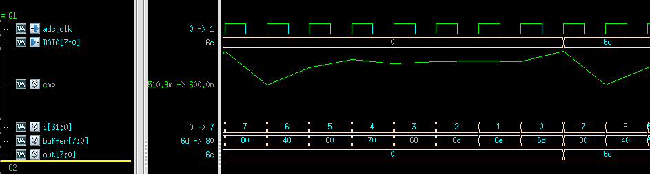
To test the verilog-AMS model, a constant 0.51V was applied to the input. At each clock edge, the sampled value is compared to ''cmp'' which is effectively the DAC output. This DAC output is generated from the value in 'buffer'. It can be seen from this model, that after 8 clock cycles the output is captured as 0x6C, which for a 1.2V full scale ADC gives a corresponding voltage of 0.50625 V, just below the applied 0.51 V.
Over the APB Interface the read output is 0x6C, confirming that both the ADC model works, and that APB register access is working as expected
Physical Design and Verification
The physical layout and verification of the ADC's individual subsystem is currently under development (as on November 2024). The first, and most complex, component is the Op-Amp. Physical design involves placing the fundamental components from the technology node PDK (transistors, resistors, capacitors etc.) and routing the nets to connect these components.
Once a layout is complete, verification takes place. First is the Design Rule Checks ("DRC") and Layout Versus Schematic ("LVS"). DRC checks the layout against the design rules from the foundry, and LVS checks the layout against the prior design stage higher level abstract representation (eg. netlist) to check that they are both equivalent. During the layout process we also add dummy devices which are placed to improve the uniformity across the device, as devices at the edge of a geometry are likely to be slightly distorted compared to the centre. Usually this applies to things like gate thickness and dopant profiles.
Mixed Signal Verification
Currently the mixed signal component under development has been tested as a separate entity. The digital side being tested using a simplified verilog-A model. Verilog-A is the analog-only subset of Verilog-AMS hardware description language. Verilog-A has been used to describe primitive circuit components (resistors, capacitors etc.) that a SPICE class simulation tool uses to build up a system of nonlinear differential equations that are solved when the simulation is executed. , The analog side is being tested with basic digital switches, but not with the full control system expected for the final project delivery.
Design and validation testbench
To be added
First working version
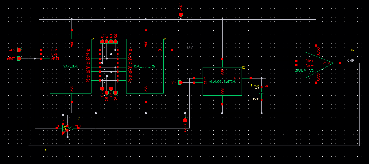
A first version of the ADC's schematic is shown above. A detailed schematic of each of the components will be added at a later date.
For a first iteration it (sort of) works. The implementation uses the same opamp used in the DAC for the comparator. The working principle is after a active low pulse on the nRST pin the analog switch + capacitor will hold the value of Vin at that time and pass to the comparator. The SAR begins with the MSB high, and all other bits low. The DAC converts this to an analogue signal and compares against the held version of Vin. If V_DAC is greater than Vin, the comparator output will be low, and the SAR will de-assert that bit in the next clock cycle (and vice versa if V_DAC is smaller than Vin). On the next clock cycle, the MSB-1 bit will be asserted and so on until the lowest bit is reached (8 bits, 8 cycles) The value of Q will then not change until another nRST is asserted.
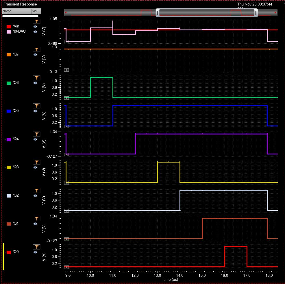
The above illustrates the behaviour defined in the expected simulation result. However it also shows that there is some error in the final DAC value. In this example a Vin of 800mV has been used, and the DAC output is 812mV. Given the binary output on Q (10110110), for an ideal DAC, this should actually correspond to 853 mV. An error of over 53mV (equates to 11.3 LSBs).
The power consumption is also higher than would be ideal.
| Total Average Power (mW) | 4.47 |
|---|---|
| SAR Average Power (mW) | 0.013 |
| DAC Average Power (mW) | 4.31 |
| Sample and hold Average Power (nW) | 2.23 |
| Comparator Average Power (mW) | 0.15 |
From the breakdown above it is clear most significant usage of power is in the DAC.
The very simplistic opamp used here has a common-mode input voltage range of about 0.3-1.2V. This directly correlates to what the comparator can "see" as a difference in the DAC output and Vin. So the actual conversion range of this ADC is only 0.3-1.2.
Comparing to the initial specification, the results of the initial implementation are:
| 8 bit resolution | Pass |
| 100 kHz sampling rate | Pass |
| 0-1.2V conversion | Fail |
| Low differential nonlinearity and integral nonlinearity | Somewhat Fail |
| Low power (<1mW) | Fail |
The conclusion of this first iteration, is that the SAR and sample & hold circuitry are working, but the DAC and comparator need more work.
Version 2
The second iteration of this design focuses heavily on:
Increasing the common-mode input voltage range of the comparator
Decreasing the power consumption of the DAC
Ideally reducing the error in the DAC conversion
The issues with the conversion range and non-linearity both mainly stemmed from the same issue, the comparator. In version 1, the same opamp used in the DAC was used in the comparator. This opamp does not have a very high slew rate, and is also a single n-channel input stage which meant that the common mode input was between about 0.3-1.2 volts. This circuit was replaced by a StrongArm comparator found here. The length of the transistors in this design were increased which seemed to improve the differential voltage down from 30 mV (as reported in the paper) to about 500uV.
To improve power consumption, the main focus was the DAC. This is a simple R-2R DAC, most of the power is dissipated through the resistors. So all that was needed was to increase the resistance of these to produce a large decrease in the total power consumption. The downside of the increase to the resistance is a reduced the width of the resistors which makes them more susceptible to manufacturing variation, however it does have the added bonus of reducing the overall area.
The conversion error now looks as below based on simulations with a voltage input from 0-1.2V in steps of 2mV
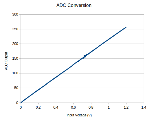
The above shows the conversion is very linear except around the 0.7-0.8V range. Whilst this isn't ideal it is acceptable for this version 2, It may be further investigated later to see if it can be improved. The error (in LSBs) for the range of input voltages is shown below:
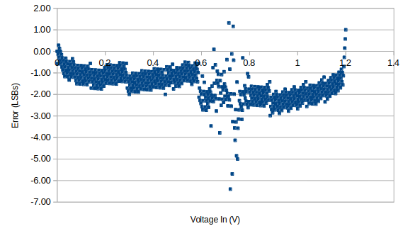
The maximum error is at about 0.78V with an error of -6.3 LSBs. The average error is -1.56 LSBs.
| Total Average Power (uW) | 571.7 |
|---|---|
| SAR Average Power (uW) | 1.47 |
| DAC Average Power (uW) | 570.2 |
The table above shows that the total power has been reduced significantly and can now met our specification of less than 1mW power consumption.
In terms of sampling rate, it still meets the spec of 100 ksps sampling rate. This could be improved to about 12.5 Msps although errors increase slightly as sampling rate is increased. A full investigation has yet to be completed.
Multi-corner simulation was run at tt, ff, and ss corners from -40 to 85C. This has also not been fully investigated yet but only a 1 LSB variation is seen across these corners so this works reasonably for now and will be investigate further at a later date.
Project Milestones
Do you want to view information on how to complete the work stage ""
or update the work stage for this project?
-
Behavioural Design
Design FlowTarget DateDesign of the components of the Analog-digital converter
-
Behavioural Modelling
Design FlowTarget DateModel the analog behaviour of the subsystem and confirm it meets the requirements
-
Mixed Signal Simulations
Target DateSimulation of the full mixed signal subsystem
-
Integration with nanoSoC
Target DateIntegration of the top level interface within nanoSoC with mixed signal simulations
-
Physical Design
Design FlowTarget DatePhysical design of ADC
-
Physical Verification
Design FlowTarget Date -
Mixed Signal verification
Target Date
Team


Additional Project for:
 Daniel Newbrook
Digital Design Engineer
at University of Southampton
Research area: IoT Devices
ORCID Profile
 Cortex-M0
 Advanced Microcontroller Bus Architecture
Submitted on
Comments
Power Management to enable measurement of energy consumption
There have been some recent discussions of how to improve the design of nanoSoC to enable finer power management of parts of the system to enable more precise measurement of energy consumption.
It would be interesting to understand the potential for the sensor subsystem. One option might be to have a power management function that distributes the AHB clock to only a selected set of peripherals where the external environment can determine the set to select. This might be configured as part of the SoC startup or perhaps as masks that can be set at run time to distribute the clock to a limited number of selected peripherals.
There was some discussion on whether to use simple registers to keep the gate count low, as is a key driver for nanoSoC or to use a specific power management controller.
Any power management design may need to consider what other considerations need to be taken, for example, any voltage regulators that can be set to run in low-power mode, if any of the sensor system needs some energy even in an idle state.
The interrupt mechanism that causes the re-selection of the peripheral device to return to active operation and any latency associated with this action.
Integration with nanosoc
Although the actual work of Integration with nanosoc comes later in the milestone I feel we should complete the Architecture definition as soon as we can. This will help contestants in the educational/collaboration track with their own Architecture definitions.
Tutorials
Hello John,
I need some tutorials to help me with approach to progress in my design.
Thank you and kind regards,
Progressing
Hi Ayodeji,
I think from the front end side, the best place to start is to consider what kind of sensors you want to connect to, and what requirements they have. Particularly - voltage range, input type (single ended or differential are most common), are they active or passive, how frequently you want to read the sensor, and what digital resolution you need.
I think once you have this information you can start thinking about what the requirements are on the analog front end. For instance if you have a differential input, you will need some sort of differential amplifier that feeds into the ADC.
Once you have done this if you could add this information on your project we can continue to assist you there
We will make this work public on the accelerator project repository shortly, I'm just trying to get it working in a way that doesn't break the digital only flow, so you can possibly integrate this into your design as well
Daniel
Add new comment
To post a comment on this article, please log in to your account. New users can create an account.