FPGA-Powered Acceleration for NLP Tasks
Project Overview:
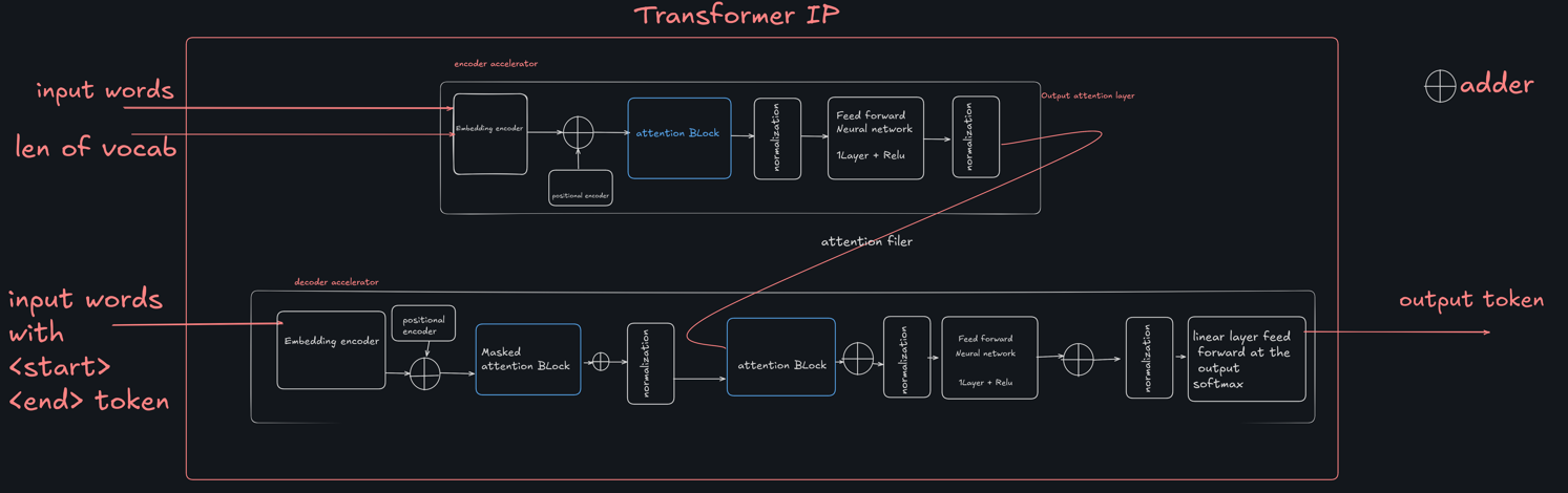
Natural Language Processing (NLP) transforms how machines understand and interact with human language. Whether predicting the next word in a sentence, translating languages in real-time, or understanding contextual information from a body of text, NLP applications are increasingly prevalent in various fields such as virtual assistants, translation services, and automated customer support. To meet the growing demand for efficient and real-time NLP processing in embedded systems, we propose designing and implementing a Tiny Transformer Intellectual Property (IP) core. This core will be integrated with an ARM Cortex IP, leveraging the strengths of both the processor system (PS) and programmable logic (PL) parts of a System on Chip (SoC) to create a highly efficient solution for real-time NLP tasks.
Objectives:
1. Design and Implementation of Tiny Transformer IP:
- Develop a compact and efficient transformer IP core using high-level synthesis (HLS), tailored for resource-constrained environments.
- Include essential components such as an encoder, decoder, attention blocks, normalization layers, and feed-forward neural networks.
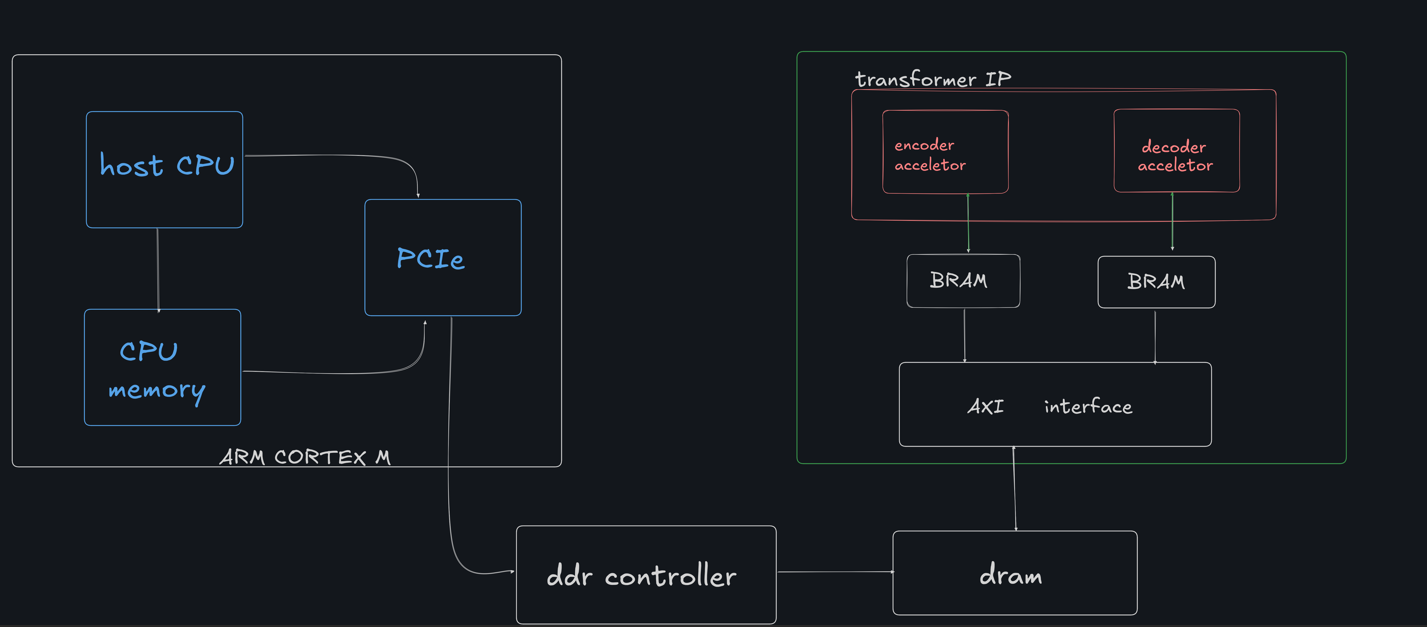
2. Integration with ARM Cortex IP:
- Utilize the ARM Cortex IP as the processing system (PS) for handling high-level control and preprocessing tasks.
- Integrate the Tiny Transformer IP as the programmable logic (PL) part to accelerate computationally intensive transformer operations.
- Establish seamless communication between the PS and PL using the AXI interface.
3. System Architecture Development:
- Implement a host CPU that interacts with the Tiny Transformer IP via PCIe and manages data flow.
- Integrate BRAM for intermediate storage and a DDR controller for main memory access.
- Optimize the data path and memory hierarchy to ensure low-latency and high-throughput processing.
4. Performance Evaluation:
- Benchmark the integrated system against conventional CPU-only implementations to demonstrate improved performance.
- Assess power consumption and resource utilization to validate the efficiency of the Tiny Transformer IP in embedded scenarios.
Expected Outcomes:
The successful completion of this project will result in a highly optimized Tiny Transformer IP core integrated with an ARM Cortex IP. The project will generate a complete RTL to GDSII flow, enabling the tape-out of our accelerator on a 65nm technology node. This integration will provide a robust solution for deploying transformer-based models in resource-constrained devices, enabling real-time processing of NLP tasks with significantly reduced latency and power consumption. This advancement will pave the way for sophisticated applications in IoT devices, edge computing, and mobile platforms, making advanced NLP capabilities more accessible and efficient.
Project Milestones
Do you want to view information on how to complete the work stage ""
or update the work stage for this project?
-
Architectural Design
Design FlowTarget DateCompleted DateProject Kickoff:
- Define project objectives and scope.
- Review existing technologies and research relevant to Tiny Transformers and ARM Cortex integration.
-
Behavioural Design
Design FlowTarget DateCompleted DateDesign Phase:
- Develop initial architecture for Tiny Transformer IP.
Begin high-level synthesis (HLS) of essential transformer components (encoder, decoder, attention blocks).
-
Behavioural Design
Design FlowTarget DateCompleted DateImplementation Phase:
- Complete HLS of Tiny Transformer block components of input embedding.
- Develop communication protocols between PS and PL parts of the SoC.
-
Behavioural Design
Design FlowTarget DateCompleted DateSystem Architecture Development:
- Implement attention block and normalization block.
-
Accelerator Design Flow
Design FlowTarget DateCompleted Dateimplemented encoder block with hardware utilization as 22 % LUTS and 7 % BRAM.
-
Milestone #6
Target Date -
Milestone #7
Target Date -
Milestone #8
Target Date -
Milestone #9
Target Date -
Milestone #10
Target Date -
Milestone #11
Target Date -
Milestone #12
Target Date -
Milestone #13
Target Date
Team
 Project Creator
at Indian Institute of Technology Jodhpur
![]() Accelerators
Accelerators
![]() Hardware design
Hardware design
![]() Accelerator Design Flow
Accelerator Design Flow
Submitted on
Comments
Updates to milestones
Hi,
We are excited for 2026 and have many exciting things planned for the year. As I understand the project you are working through some Behavioural design using both simulation and trying to deploy to an FPGA environment.
I think you have been working on the integration of the NanoSoC M0 reference design with your own custom accelerator. You have been using the example AES-128 project. You have been using the GCC compiler. We had not done enough verification on the core reference design with this compiler and an error was found and reported and Daniel has fixed this in the git repo so you could progress. The problems are causing some issues in the firmware that is supposed to run in the M0 controller to handle the data transfers to and from the custom accelerator.
It looks to me that you are already working on the Simulation milestone but it is not listed in the Project Tracker.
It should be simple to add this, just click on the 'Simulation' link in the tracker.
You can view the information on the design flow stage and update your milestone to say you have started this.
It would be great to keep the milestones updated so we can help as best we can.
John.
Query regarding interfacing ARM soc with accelerator
I have been working with PYNQ Xilinx and with Zynq-7000 IP to implement an accelerator using memory-mapped AXI interfaces between the PS and PL parts of the SoC.
I would like to understand how to interface my accelerator with the SoC architecture in this new setup. Specifically:
1) How can I replicate the memory-mapped AXI communication approach that I used on the FPGA in an ASIC flow?
2) Which Arm SoC would be apt and what will be the procedure to interface the Soc with the custom accelerator
3) What modifications are needed to efficiently integrate the accelerator with the SoC's memory and CPU subsystems?
4) Which SoC would be most suitable for integrating a custom accelerator, ensuring good support for AXI interfaces, data transfers, and power/performance optimizations?
5) How can I replicate the memory-mapped AXI communication approach that I used on the FPGA in an ASIC flow?
6) What modifications are needed for efficient integration of the accelerator with the SoC's memory and CPU subsystems?
Additionally, I am familiar with HLS tools like HLS4ML and frameworks like TensorFlow for developing accelerators but they don't support transformers right now.
We are okay to schedule a video call as per your convenience regarding the interfacing of ARM Soc with the accelerator
Query regarding interfacing ARM soc with accelerator
Hi,
Each of our reference SoC's are at different development stages, so this will also depend on your timeline. If you want something ready to go very quickly I would suggest looking into nanoSoC
Back end integration with SoC to move beyond FPGA implementation
You might like to look at the two pages on TensorFlow and HLS4ml that are in the interests section on maching learning.
Currently you have been looking at 'Develop communication protocols between PS and PL parts of the SoC' but when you move to the full ASIC flow the PS part needs to be replaced by the actual SoC infrastructure.
Do you need some help with this? We would be happy to have a video call if that would help?
FPGA Prototyping
Prototype with Zynq: We'll start by prototyping the IP on the Zynq MPSOC FPGA with integrating HLS generated IP with the Zynq and other IP .
PYNQ Overlay: Create a PYNQ overlay for easy design space exploration and benchmarking.
Application Testing: Run the application to evaluate performance and make necessary adjustments.
This approach will allow us to iterate quickly and gather critical insights before moving to the physical design process.
As of now the model size is quite large in MB's so we are trying to reduce the model size using some techniques and want to know what should be the ideal model size. We should be good to go as there would be some trade offs in accuracy ?
Transition from FPGA to System on Chip design
Following up the comments from John D, I suggest there are three distinct phases for this project:
The project proposal as it stands I think would be very hard to fully complete successfully within a limited time (and budget) if the assumption is simply to map the transformer and memory system architecture to a 65nm process technology(?)
Transition from FPGA to System on Chip design
As you develop the design options for the communication protocols between various parts of the SoC you should consider the necessary SoC infrastructure beyond the FPGA implementation when the project moves towards the stages that will 'generate a complete RTL to GDSII flow, enabling the tape-out of our accelerator on a 65nm technology node'.
In later stages there is no separation between PS and PL parts. The operational characteristics of BRAM are different than those of actual on chip 65nm SRAM blocks. In the diagram above the interaction between the DRAM (do we assume this memory is off chip, not on the same ASIC die as the main system?) and the memory (SRAM blocks) close to the transformer IP needs a clearer data movement strategy for the SoC. The current taped out nanoSoC designs on 65nm mode using nanoSoc reference design considers for small data volumes and small accelerators the on chip SoC architecture and has used a variety of DMA approaches. Depending on the model sizes you are planning a more capable architecture may be required. You might want to look at last year's entry from IITH and the comment I made about on chip memory requirements.
I hope this helps.
Memory requirement
On chip memory is a critical aspect of SoC area/cost. A recent paper on Optimizing the Deployment of Tiny Transformers on Low-Power MCUs considered the issue of high memory footprint of intermediate results and frequent data marshaling. The paper discusses the issue of memory constraints and techniques for data movement such as the use of Direct Memory Access.
If you can provide some idea of data sizes and movement requirements it will help.
Related to project
Prototype with Zynq: We'll start by prototyping the IP on the Zynq MPSOC FPGA with integrating HLS generated IP with the Zynq and other IP .
PYNQ Overlay: Create a PYNQ overlay for easy design space exploration and benchmarking.
Application Testing: Run the application to evaluate performance and make necessary adjustments.
This approach will allow us to iterate quickly and gather critical insights before moving to the physical design process.
As of now the model size is quite large in MB's so we are trying to reduce the model size using some techniques and want to know what should be the ideal model size. We should be good to go as there would be some trade offs in accuracy ?
Architectural Design
This item on Cortex M voice solutions might be useful in determining the system requirements and some of the decisions needed in establishing the SoC Architecture.
Breaking down the processing to core parts such as inputs and data requirements of the ML processing to identify system resource requirements.
The data transfers for input and model through the system.
There are some approximate figures, "minimum of 300KB for model storage (assuming
100s of domain specific utterances)". Do you have any views on model sizes and through put?
We look forward to hearing from you.
Sizing potential system design to natural languages models.
It was good to have the call today and discuss the project. It was helpful to discuss the specification for the project as well as progress on the development of your model and activities to reduce the size of the model for inference on the edge. As we discussed the small microprocessor SoC reference design such as nanoSoC are perhaps capable of keyword detection tasks with a mid-range SoC reference design using specific acceleration subsystem can handle more demanding speech recognition tasks. Hopefully this diagram from the ML Developers Guide for Cortex-M Processors and Ethos-U NPU is helpful in visualising the types of ML application.
Copyright © 1995-2024 Arm Limited (or its affiliates). All rights reserved
As we discussed it is not only the computational intensity of the specific ML application but the size of the model and movement of data representing the model within the system both the System on Chip memory and the external off chip memory demand.
Larger language models
We also discussed the option for deploying the model on the Corstone 300 Fixed Virtual Platform with the ability to separate parts of the model compute to the Ethos-U NPU or the M class CPU in an optimal way.
LiteRT is the new name for TensorFlow Lite (TFLite) which is a portable runtime for executing models from a number of AI/ML frameworks including TensorFlow. Without optimisation the runtime would use portable Reference C Kernels. Arm provides kernels optimised for it's processors in the CMSIS-NN library. Some operations can be highly optimised by execution within the Ethos-U accelerator. Velo takes a portable model and changes it to request the runtime to use the most efficient Arm compute infrastructure.
A baseline might be established by taking your model and seeing if it can be effectively executed on the M55/U55 combination using a Fixed Virtual Platform as a simulation environment.
Welcome to SoC Labs
Thank you for submitting this project, it looks very interesting and I look forward to hearing more about it.
If you need any help, just add a reply here and we will see what we can do to help.
We look forward to hearing from you.
Tiny-Trans
Team Members:
Abhishek Yadav (yadav.49@iitj.ac.in)
Ayush Dixit (m23eev006@iitj.ac.in)
Binod Kumar (binod@iitj.ac.in)
Add new comment
To post a comment on this article, please log in to your account. New users can create an account.