Basic PLL with TSMC 65nm
To design and verify a simple PLL for use as generator of clock signals in System on Chip design. The desired outcome from this project should be the following:
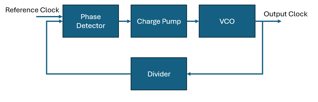
- Clock generation for frequencies between 60 MHz and 1.2 GHz
- Include PLL-lock signal for system start up
- Low clock uncertainty below 5% (transition time and jitter)
- Integer clock divider which can be updated at run time
- Minimal area
The resulting IP for these component blocks will be made available to the soclabs community for the upcoming design contest.
Collaborators who have an interest in helping develop this IP especially those with experience with analog and mixed signal design are asked to make contact by simply joining this collaboration project (see the button on the right --> )
Background
Phase-Locked Loop (PLL) are used in System on Chip implementations to control the quality and supply of clock signals. PLLs can be used to to drive internal clock trees that allow parts of the System on Chip to operate at different frequencies. A design may use more than one PLL with PLL designs varying in their range of frequency, power, area, performance, and additional functionality. One critical characteristic is Period Jitter which is a concern for Static Timing Analysis. Other concerns can be long term jitter for communication synchronisation and data movement. PLL jitter is mainly determined by VCO performance. PLL design can make various trade off between power, area and control of noise, etc. and can be optimised for specific System on Chip applications.
Initial design
The current project plan is to base the PLL design on the git project - Analog-Design-of-1.9-GHz-PLL-system by user muhammadaldacher. Credit goes to them for the initial design although some changes have been made to the subsystems. The same FET parameters have been used (width, length and multiplicity of transistors) although the original design was for a 90nm technology node and parameters need to be re-optimised for this project's target of 65nm node. The original project targeted specifically a 1.9 GHz operating frequency whereas this project aims to create lower frequencies < 1.2 GHz.
Design and test of sub system blocks
Each block has been implemented and tested separately. Basic functional verification has been done to ensure the blocks work. Once integrated more in depth characterisation of the blocks will be required to optimise the system as a whole.
Op-Amp
This has been fairly heavily modified from muhammadaldacher's design. A second stage has been added to this opamp to improve open loop gain, hopefully this can be reused as a simple opamp in other designs as well. Testbench for simulation was with opamp in open loop mode, tying negative input to 1/2 VDD (600mV) and supplying an AC signal to positive input with a DC offset of 1/2 VDD. Results from simulation are:
- DC Open loop gain : 61.72 dB (1220 absolute gain)
- Unity gain frequency : 239.5 MHz
- Phase margin : 19.67 degrees
- Bandwidth : 485.2 kHz
VCO
A current starved ring oscillator has been chosen for simplicity. An initial implementation of the LC-VCO indicated the inductors for this would design choice would take up a fairly significant area and this project aims to limit the area used as much as possible for low cost minimal area System on Chip designs. The chosen design is a simple 7 stage inverter ring oscillator with an output buffer stage. Testbench for simulation effectively had a triangle wave input to sweep the input voltage from 0V to VDD (1.2V)
- Frequency range 16 MHz to 1.4 GHz
- Control voltage from 0.4 to 1.2V
- Rise time @1.4 GHz = 10.2 ps (slew 69.9 V/ns)
- Fall time @1.4 GHz = 12.6 ps (slew 56.8 V/ns)
Divider
A simple 2^N divider is implemented. The project aims to replace this block entirely so that the design can set an n-bit register with an integer divider to generate a larger selection of output clocks.
PLL sub-system integration tests
Initial tests of the subsystem with a reference clock frequency of 30 MHz and divider of 8 to give a clock frequency of 240 MHz. These values were chosen for the initial test as the clock frequency of current nanosoc design using TSMC 65nm node is 240 MHz and we future nanosoc implementation may replace the external clock with this PLL.
The settling time to within 10% of 240 MHz is 9.5 us, and to within 1% is 22.6 us
Period Jitter
- after 10 us: +/- 375 ps (9% period)
- After 20 us: +/- 59 ps (1.4% period)
- After 25us: +/- 27 ps (0.6% period)
More in depth characterisation of the PLL performance over a wider range of frequencies is required to ensure broader use for SoC development.
Project Milestones
Do you want to view information on how to complete the work stage ""
or update the work stage for this project?
-
Basic System test and integration
Target DateCompleted DateDesign and simulate the basic components of the PLL and test the full subsystem together
-
Check/replace component choices
Target DateInitial design is based solely on the most basic components but the TSMC 65nm PDK has a wide range of choices for components, some of which may be better suited
-
Optimise Component parameters
Target DateOptimise the component parameters: particularly the width and length of transistors but also chosen values for resistors and capacitors
-
Layout
Target DateConvert from schematic design to physical layout, and then resimulate
Team

Additional Project for:
 Daniel Newbrook
Digital Design Engineer
at University of Southampton
Research area: IoT Devices
ORCID Profile
![]() RF and Analog Design
RF and Analog Design
![]() Hardware design
Hardware design
Submitted on
Add new comment
To post a comment on this article, please log in to your account. New users can create an account.