DRAM Controller integration in megaSoC
To enable full operating system support in megaSoC, a substantial amount of memory is required to accommodate the complexity of modern Linux-based software stacks, including the kernel, drivers, middleware, and user-space applications. Linux environments, unlike lightweight bare-metal systems such as nanoSoC, demand not only larger memory footprints but also consistent access to high-bandwidth memory to maintain performance across multitasking workloads. The most common approach is to incorporate external DRAM, which offers the necessary capacity and throughput. The use of DRAM enables the system to handle everything from file systems and networking to graphical interfaces and real-time data processing. Integrating a DRAM subsystem is non-trivial, challenge requiring the design and validation of a memory controller and physical interface (PHY) that can meet strict timing, signal integrity, and power constraints. A DRAM subsystem adds considerable complexity to the overall SoC design, both in terms of hardware implementation and system-level verification.
SoC Labs is very fortunate and thankful to Synopsys for providing access to their IP's for this project. They have supplied the Enhanced Universal DDR Memory Controller (uMCTL2) and their LPDDR4 multiPHY. Using these pre-verified IP's, should allow megaSoC to be a high-performance system with full OS support.
Specification
Before agreeing the appropriate IP with Synopsys a specification of the megaSoC system needs was developed. This enabled clear choses for the right IP for the project. The specifications included:
- Memory Type : LPDDR4
- This was chosen as we wanted megaSoC to emulate something like the Raspberry Pi or other single board computers.
- Speed: up to 2Gb/s
- We aren't targeting top-of-the-line computation, (otherwise we would probably go for LPDDR5). megaSoC needs enough bandwidth for reasonable applications to run.
- Bus Interface: AXI 4
After discussing with synopsys, out requirements vs. their available IP, we came to the agreement of using the uMCTL2 and LPDDR4 multiPHY.
Configuration
The IPs have a significant number of configurable options, each which add complexity to the design and verification effort.
Integration
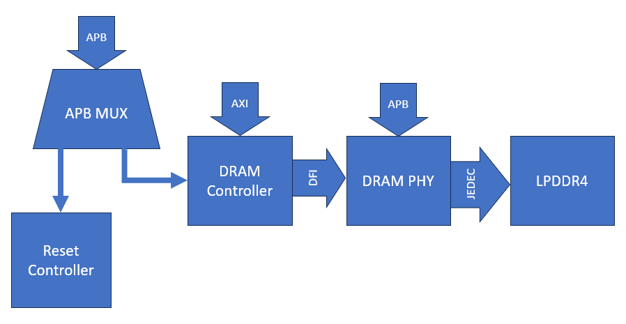
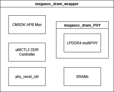
The design hierarchy is shown below. The top level wrapper includes a generate statement to allow for the inclusion of the Synopsys IP (or to not use it if users don't have access)
The main integration points are:
- Reset + clock control (including APB interface)
- APB interface on uMCTL2 and multiPHY
- AXI to uMCTL2
- SRAMs for PHY (this has a small CPU core to run the training algorithms)
- SRAMs for controller (buffers for write data)
- DFI interface between controller and PHY
- PHY to pins
- Interrupts
Other integration points that we are currently not focussing on:
- Scan interface to controller
- ATPG interface to PHY
- Bypass interface to PHY
All of these integration points need to be verified.
Verification
See the accordion below for all of the verification points
- Reset Controller
The reset controller is a small bit of custom IP to assert or de-assert the reset and power-ok pins
The address map for this is:
- 0x00 (bit 0) - ddrphy_reset
- 0x04 (bit 0) - ddrphy_pwrok
- 0x08 (bit 0) - ddrcore_rstn
This allows for independent control of all 3 signals. Further additions could be made to add things like clock enables for the IP
We need to verify the control of each of these 3 signals
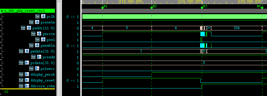
Looking at the above graph we can see
- after presetn - registers are default values (all zeros)
- At M1 - write to 0x00 sets ddrphy_reset high
- At M2 - write to 0x04 sets ddrphy_pwrok high
- Before M3 write to 0x00 to set ddrphy_reset low
- At M3 - write to 0x08 to set ddrcore_rstn high
- At M4 write to 0x04 to set ddrphy_reset high
As a very simple IP, this shows the working principle.
- APB interface on uMCTL2 and multiPHY
APB read and write to the controller and PHY is needed to control their behaviour
This one is fairly straightforward. We added an APB interface to the main system bus of megaSoC and can run read and write commands to the PHY and controller successfully
TO NOTE - the PHY data/address alignment was not to 32 bits. We had to shift the addressing by 2 so that the system bus / CPU could properly access the registers for 32 bit word aligned accesses
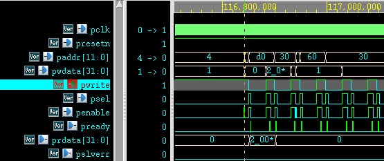
- SRAMs for PHY
The SRAMs for the PHY are used to program the PHY training routines. There is an instruction memory and data memory
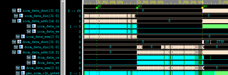
Looking at the above waveforms you can see
- M2 - programming iccm (instruction memory)
- M3 - programming dccm (data memory)
- M4 - boot started for the PHY training. Reading from iccm and dccm
Whilst this does not fully verify the behaviour of the SRAMs. This shows that they can be programmed and read from by the PHY to run the training program.
- SRAMs for controller
Currently, we would only be able to observe this behaviour once the subsystem is running AXI write transactions and we have not yet got that working. For now this is on hold.
- DFI interface between controller and PHY
Our first approach at this was test this using AXI based transactions. This would mean that the DFI interface is tested by functionally. However, getting it to the point of running AXI transactions is currently not working. We suspect that this is in the configuration of the PHY init training software but we can't be fully sure that it is not a problem in the DFI interface.
The slight complexity here is that the controller has a single DFI interface, but the PHY breaks it up into phases, so you have to select which bits from the controller correspond to the correct phases in the PHY. These phases are needed because of the ratio in clocks between the phy and controller (typically either 1:1, 2:1, or 4:1)
What we are currently trying to do is add a monitor that sits between the controller and PHY to ensure correctness of the connections. This monitor comes from the VC - VIP portfolio from Synopsys, we can add a UVM component to monitor signals here.
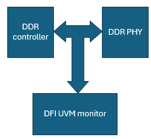
The idea is shown above, but currently this is not finished work
- PHY to pins
Check connection from PHY to pinout in testbench. This will be verified by checking that the target device in the testbench is recieving values from the DDR multiPHY.
- AXI to uMCTL2
After training and initialisation is complete, we should be able issue AXI requests to read and write to the DRAM. Currently we are stuck on the training and init phase.
- Interrupts
Not yet decided how to test these
Update on PHY verification (12/05/26)
After discussing with synopsys, one issue they raised is that maybe the problem with the PHY interacting with the device in the testbench is that the device is not setup correctly. I was using the synopsys VIP for the LPDDR4 device and what we could see from the simulation environment was as below
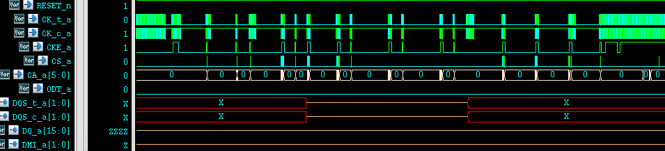
With this we can see that the PHY sets the DQS pins to Z's, this looks like the PHY is expecting some response from the device but isn't recieving it. We can also see some activity happening on the CA pins that look like it's trying to initialise the device.
If we replace the Synopsys VIP with an LPDDR4 model from micron we instead see this:
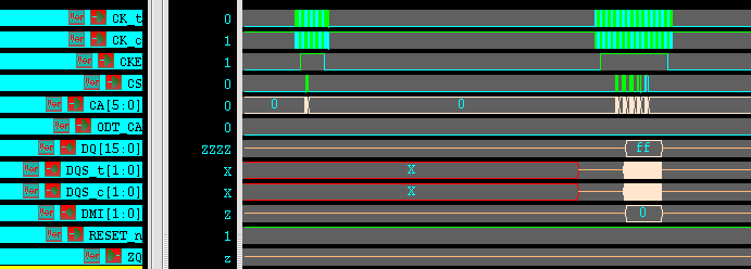
This is much more of what we expect. Unfortunately the model from micron is really designed to be tested at full speed (i.e. timing must be adhered to for pulse widths etc.) This also doesn't work to completion as the log shows below:
PU-CAL = VDDQ/3 @ FSP_WR = L
PPRP mode disable.
PDDS = RZQ/1 @ FSP_WR = L
Fast response (high current) mode (VRCG = H)
Frequency set point[0]
Normal operation (MR13 OP2 = L)
PU-CAL = VDDQ/3 @ FSP_WR = H
PPRP mode disable.
PDDS = RZQ/1 @ FSP_WR = H
DQ_ODT = RZQ/3 @ FSP_WR = H
CA_ODT = RZQ/3 @ FSP_WR = H
 Vref_CA_Range = 1'b1 and Vref_CA = 6'b001101  set @ FSP_WR = H
 Vref_DQ_Range = 1'b0 and Vref_DQ = 6'b101011  set @ FSP_WR = H
SoC_ODT Disable @ FSP_WR = H
ODT-CK  = 1'b1
ODT-CS  = 1'b1
ODT-CA  = 1'b0
PPRE mode disable.
No offset, 5 C gradient ( MR4_OP[6:5] ).
TRR mode disable
Fast response (high current) mode (VRCG = H)
Frequency set point[1]
Normal operation (MR13 OP2 = L)
Error: megasoc_tb.g_ddr_model.u_lpddr4_dram1.ins_1ch.PROTECTED 4169238 ns   MRW_2 command is illegal input.
Normal operation (VRCG = L)
Frequency set point[1]
Normal operation (MR13 OP2 = L)
Error: megasoc_tb.g_ddr_model.u_lpddr4_dram1.ins_1ch.PROTECTED.task_lpddr4_MRW_2_command_check 4174252 ns  MRW_2 command need to input consecutively after MRW_1 command input.
Whilst using this model will be very useful to check the final functionality of the DDR controller and PHY, the simulation times will take too long whilst development is ongoing. The good news from this is that we think the PHY is starting to work correct but have identified a problem in the model. Next steps are to try and fix the VIP setup so that this will work correctly.
Project Milestones
Do you want to view information on how to complete the work stage ""
or update the work stage for this project?
-
RTL Verification
Design FlowTarget DateVerify the functional behaviour of the controller and PHY working together
-
IP Selection
Design FlowTarget DateCompleted DateResult of WorkAfter discussing with synopsys the IP needs, they have suggested the uMCTL2 and LPDDR4 multiPHY
-
Verification Methodology
Design FlowTarget DateCompleted DateResult of WorkWe'll be using a mixture of UVM based components from the Synopsys VC-VIP suite, and functional verification by passing vectors from the Cortex A53 to the memory model in the testbench
-
Getting Started
Design FlowTarget DateCompleted DateResult of WorkThe scope of this project is to integrate the DDR controller and PHY. Verify the functionality. Run synthesis on the design before integrating into the hierarchical design flow for the full megaSoC
-
Specifying a SoC
Design FlowTarget DateCompleted DateResult of WorkmegaSoC is the target for this work
-
Architectural Design
Design FlowTarget DateCompleted DateResult of WorkArchitecture of the subsystem complete
-
Generate RTL
Design FlowTarget DateCompleted DateResult of WorkGlue logic for the subsystem is complete. As well as design of a reset controller for local reset behaviour
Team


 Project Creator
 Daniel Newbrook
Digital Design Engineer
at University of Southampton
Research area: IoT Devices
ORCID Profile
![]() Hardware design
Hardware design
Submitted on
Add new comment
To post a comment on this article, please log in to your account. New users can create an account.