Low-Cost and Low-Power Data Acquisition System(DAQs) for Real-time Data Collection
The development of a Low-Cost and Low-Power Data Acquisition System(DAQs). The DAQs will be made up of end-terminal and a gateway. The end-terminal will be micro-controller-driven device built on a SoC FPGA technology with built-in capability for machine learning. The end-terminal will be able to transmit and receive data using the Low Power Wide Area Networking (LPWAN) communication protocol that functions on LoRA.
LoRa is a wireless radio frequency technology that operates in a license-free radio frequency spectrum. The gateway will be micro-controller-driven device built on a SoC FPGA technology capable of supporting wireless connections to the end-terminal.
The aim of the research is to develop an end-terminal and gateway devices for the collection of real-time data from the environment.
The output of the project will be a data acquisition system consisting of IoT -based sensor, wireless transceiver and gateway. These are the work packages:
WP1. To design a micro-controller based end-terminal that will interface to a sensor. The end-terminal will be operated on low-cost controller readily available in the Nigeria. The end-terminal will operate on low-power as well. The end-terminal will provide external interface for wireless connectivity. But, the default will be the LPWAN The circuit will be designed, optimised, calibrated, and patented. It is expected that end-terminal will be (50- 60)% SoC FPGA technology.
WP2: To design a micro-controller-based gateway that will interface data captured by the end-terminal to the cloud server. The gateway will operate on low-cost controller and components readily available in Nigeria. The gateway will operate on low-power and provide external interface for wireless connectivity between itself and the end-terminal. The gateway will be configurable to interface a finite number of end-terminals. Its default wireless protocol will be the LPWAN
It is expected that the gateway circuitry will be (50-60)% SoC FPGA technology dependent. The design of the gateway will be simulated. The optimised gateway will be realised and tested. The test-run data from the gateway will be benchmarked with off-the-shelf IoT-based sensor.
Project Milestones
Do you want to view information on how to complete the work stage ""
or update the work stage for this project?
-
Architectural Design
Design FlowTarget DateRequirements Specification:
The DAQs has two modules - the Gateway and the End-terminal.
End-Terminal Requirements:
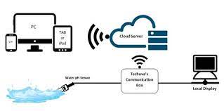
Purpose: Outdoor device for gathering real-time environment data
Inputs Power button, 5 sensor connectors:
Outputs: Antenna, 3 indicators - active, low power & power good
Functions: monitors 5 water quality parameters - PH, TDS, Temperature, Turbidity & ???; transmits
-
Decomposition and Familiarisation
Target DateDecomposition and familiarisation with the SocLab environment
Decomposing the main functional block into three parts:
- MCU - nanosoc re-usable MCU Platform,
- External Connectivity Subsystem, and
Power and Clock Management Subsystem
-
Sensor Specifications
Target Date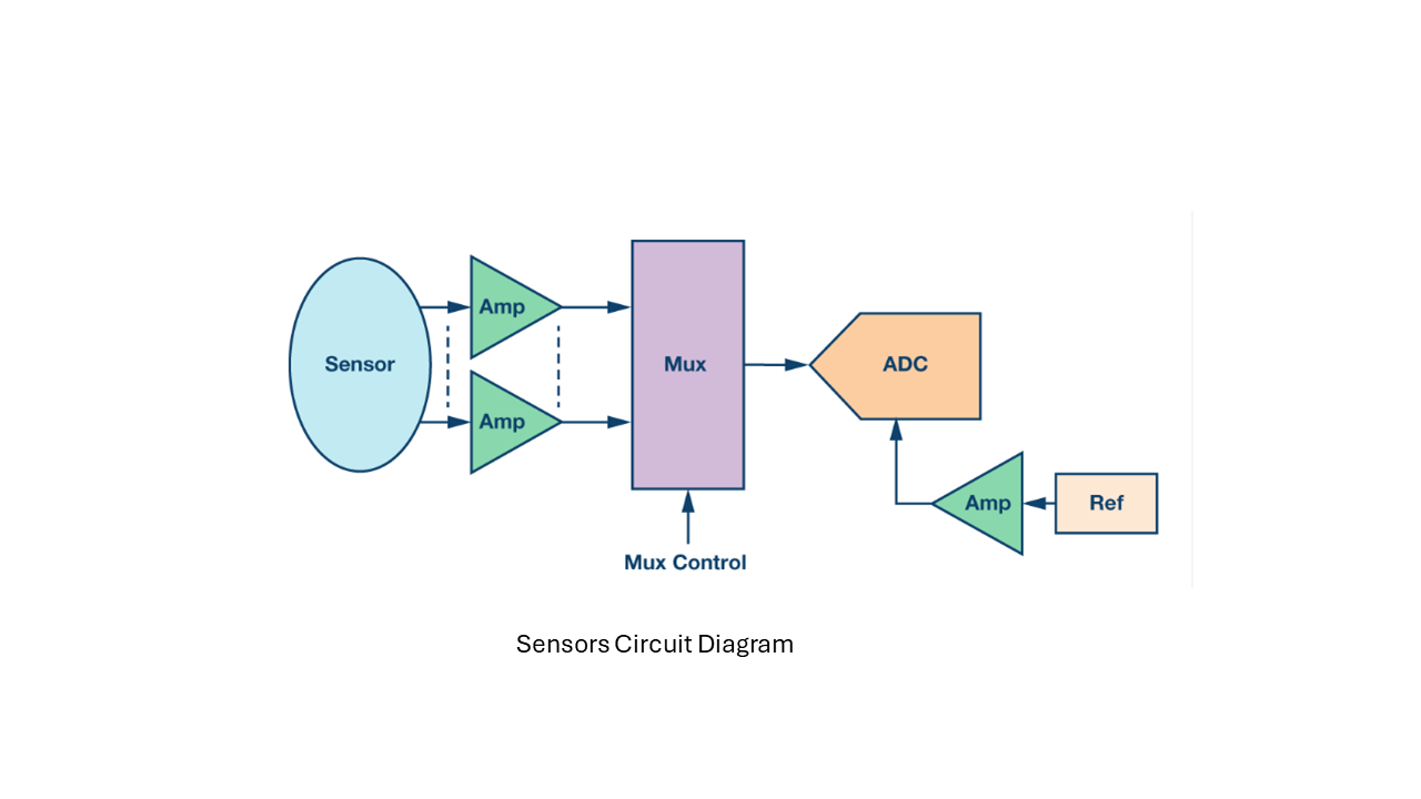 Sensor Specifications
Ph Sensor
- voltage range : 5v
- input type (single ended or differential are most common) : differential
- active or passive: passive
- sensor data refresh rate , less 5s
- digital resolution . ???
Temperature Sensor
- voltage range : 3.3v - 5v
- input type (single ended or differential are most common) : single
- active or passive: passive
- sensor data refresh rate , less 1s
- digital resolution . 9-12-bits
Turbidity Sensor
- voltage range : 5v
- input type (single ended or differential are most common) : single
- active or passive: passive
- sensor data refresh rate , less 500ms
- digital resolution . ????
-
Sensors -NanoSoC System interface
Target Date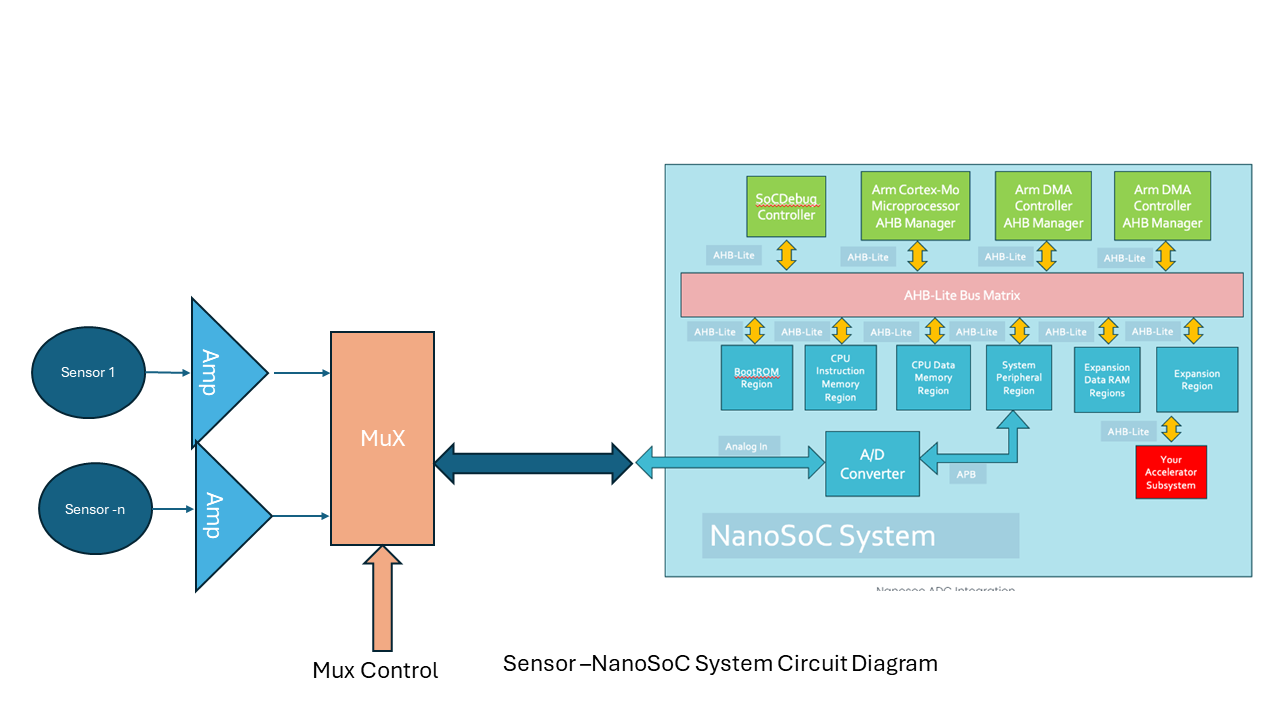
-
Milestone #5
Target Date -
Milestone #6
Target Date -
Milestone #7
Target Date -
Milestone #8
Target Date -
Milestone #9
Target Date -
Milestone #10
Target Date -
Milestone #11
Target Date -
Milestone #12
Target Date -
Milestone #13
Target Date
Team
 Project Creator
 Ayodeji Oluwatope
Faculty
at Obafemi Awolowo University
Research area: Digital Sensor
ORCID Profile
Submitted on
Comments
Hi John,My team needs to…
Hi John,
My team needs to effect some changes to the ADC integration. We have tried to reach out Daniel.
At the moment to progress, we need some guidance on the following.
1. In our current design, some functionalities like
> controlling the analog mux (CD4051) in selecting one sensor
> reading & processing the ADC output
have been delegated to the CPU.
How do we write C firmware to control the CPU? What's our entry point to do that within the Soclab Nanosoc framework.
2. The analog mux (CD4051) select pins are connected to the GPIO 0 in our design. We assumed that the GPIO 0 & 1 pins will be exposed as part of the chip. Is that correct?
3. We are near the phase of integrating our custom modules with the Nanosoc framework. Can we have a guide on how to test our implementation? Our current approach is to run `iverilog m1.v -o m1` in a terminal. When we have our modules integrated within the Nanosoc framework (say in the accelerator subsystem), our current approach might not be feasible.
In summary, how do we simulate our integration within the Nanosoc (like taking advantage of the make commands).
Thanks,
Ayodeji
Collaboration with Sydney
I am interested in the proposed collaboration.
How do I take up the collaboration to the next level?
Regards,
Collaboration with Sydney
Hi,
I think the best think would be to arrange a Teams call with Sydney, yourselves and the team here in Southampton. You are on the same time zone as Southampton so we will find a time that works for Sydney.
John.
Sydney's project
Hi,
Not sure if you have seen, but the team from Sydney have just posted their project for the competition and it shares some similar elements to what you are trying to achieve. If you want to check it out, its here: https://soclabs.org/project/sensing-precision-agriculture
Collaboration
Hi,
One of the goals of SoC Labs is to help form global collaborations. It might seem odd to have a contest where you actually work with other contestants but that is something a bit unique. about this contest, it is better to work in collaboration and to share IP blocks that are re-usable across projects.
John.
Collaboration with Sydney
Hi,
We think it will make great sense for a collaboration between you and the Sydney team. Both of you are looking to develop an SoC for environmental sensing and there will be a lot of common assets that can be shared between the projects and we can also have some joint Teams meet ups to share our expertise and experiences.
It would good to have a catch up on where you have got to and how we can help move this project along.
John.
Nanosoc Configuration + ADC
Hi,
We've just updated the nanosoc accelerator project repository, there is now a new way to configure nanosoc including how to include the ADC's.
If you go into the nanosoc_tech directory there is a file nanosoc.config. If you add text after any of the
ADC_x_INCLUDE =then the APB bus will be configured for an ADC, and the verilog-ams model of the ADC will be included (this is not synthesizable for FPGA or ASIC - we're working on making this available soon). There is also a test for the adc subsystem called adc_tests. This can be run from the nanosoc_tech directory withUnfortunately at the moment, synopsys VCS is the only supported simulator for the ADC, but we are working on this
Daniel
Sensors Specifications
I have provided three sensors specifications as suggested. Thank you.
Sensor Specs and ADCs
Thanks for adding these.
I think in terms of the ADC, a sucessive approximation registion (or SAR) ADC will work well for this. The one I have been working on at the moment is an 8 bit SAR but this can relatively easily be extended to higher number of bits if needed. Given the relatively low sampling/refresh rate, you could probably have 1 ADC module and multiplex over the different sensors (see more on this here). This would significantly reduce the area used in your design (but at the cost of a slight increase in complexity)
The voltages of your sensors will be a bit high for the ADC as the core supply voltage is only 1.2V, so you will need some external circuitry to bring the voltage down.
Hopefully this helps a bit, maybe you could use this to start a circuit diagram of your front-end, doesn't have to be perfect at this point but it would help to visualise your system
Daniel
Front-end circuit diagram
Where do I place the diagram?
Front end circuit diagram
Just in your project page. You can add updates to the main body of your project and add upload images using the top toolbar (see picture below)
Voltage range data from the sensors and Machine Learning
Hi,
It looks like the Architectural Design for the analog front end is progressing. Have you thought about the voltage range data and how that might be processed in terms of your ideas for Machine Learning?
You might want to consider that and continue the development of a full Architectural Design for your SoC. You could develop on the comment from Daniel to investigate "...nanoSoC there is a expansion region where you can integrate this, you may want to look some of last years competition projects as most of these were focused on ML/AI"
You could leave this part of the Architectural Design for your SoC for now and go into Behavioural Design for the analog front end? Let us know what you are planning and if you need any more help?
John.
Next Milestones
Architectural Design stage currently has three sub-stages:
Specifying a SoC
Work through the items needed to specify the highest level of design for the SoC.
IP Selection
Pick the IP parts from the Technology section. You might also want to think about your Project Structure and other high level Design Flow considerations.
Verification
You should start to think about how you will validate your SoC design. Creating verification and validation assests as you develop the design is a good working practice.
You should find some helpful examples from some of the other SoC Labs projects.
Happy to help and answer any questions.
Updating Milestones
We have been looking at ways to help us all keep track of progress on the projects and we have added a simple way to step through the necessary steps of the SoC design process flows.
In your project you will see it as a Red/Amber/Green status:
So the task “Getting Started” you can simply click on it and read the guidance and then update your project milestones as you go …
The “Getting Started” milestone has a task Access to IP and so that is now completed. So you can add that.
Likewise the Specifying a SoC it looks like you are making progress on that.
Looking forward to working with you as we step through the process milestones.
John.
Welcome to the contest. At…
Welcome to the contest.
At first look the micro-controller-driven device for collection of real-time data from the environment combined with built-in capability for machine learning is right on target for the contest.
It would be good to start to explain the requirements of the collection of real-time data.
Daniel has just updated the Architectural Design stage item in the work flow for
Specifying your IP | SoC Labs
You can add a milestone for the work. Edit the Project and select the milestone by typing... arch and then it auto completes the design step. Don't forget to save the change.
Adding your first milestone
Thanks for adding the first milestone on architecture design.
I was wondering how you see the decomposition of the system into parts to handle the collection of real-time data from the environment and combining that with built-in capability for machine learning. I was wondering if the external devices would sit on say the APB bus and the machine learning on the main SoC bus? You will see that for the NanoSoC reference and a few examples from contestants the custom accelerator for ML was integrated with a DMA controller on the main bus.
How do you see the main functional blocks being separated?
Hmmm ... I agree with your…
Hmmm ... I agree with your suggestions that i decompose the system into parts - collect and process real-time data. The idea of including ML capability sounds great. I am find out the appropriate location for ML.
APB bus and ML on SoC bus sounds great too. But, I am not familiar with the APB bus and I am not clear with the ML on the main SoC bus
Definitely, I will break down the functional blocks in the next review.
Resources on integration
Hi,
For the ML integration on the SoC bus, with nanoSoC there is a expansion region where you can integrate this, you may want to look some of last years competition projects as most of these were focused on ML/AI, for example:
https://soclabs.org/project/hell-fire-soc
https://soclabs.org/project/fast-knn-hardware-implementation-k-nearest-neighbours-classifier-accelerated-inference
On the APB side, APB is one of Arm's AMBA bus protocols and much simpler than the AHB or AXI protocols. It's used primarily for peripherals that only require low bandwidth and low power which makes it perfect for interfacing with peripheral.
We will soon be working on an example ADC integration in nanoSoC using the APB peripheral bus
ADC integration
Daniel has now published a mixed signal subsystem reference design project to extend the nanosoc reference design to add analog to digital conversion using the APB peripheral bus.
Hopefully this will help you with your Architectural design.
Sensors attached to the ADP bus
Daniel has now updated the mixed signal subsystem reference design project, you might want to follow that project to help you in your own Architectural Design.
Re: Architectural Design
The mixed signal subsystem created by Daniel is attractive. But, how do I consume it or adapt it to my design?
Add new comment
To post a comment on this article, please log in to your account. New users can create an account.