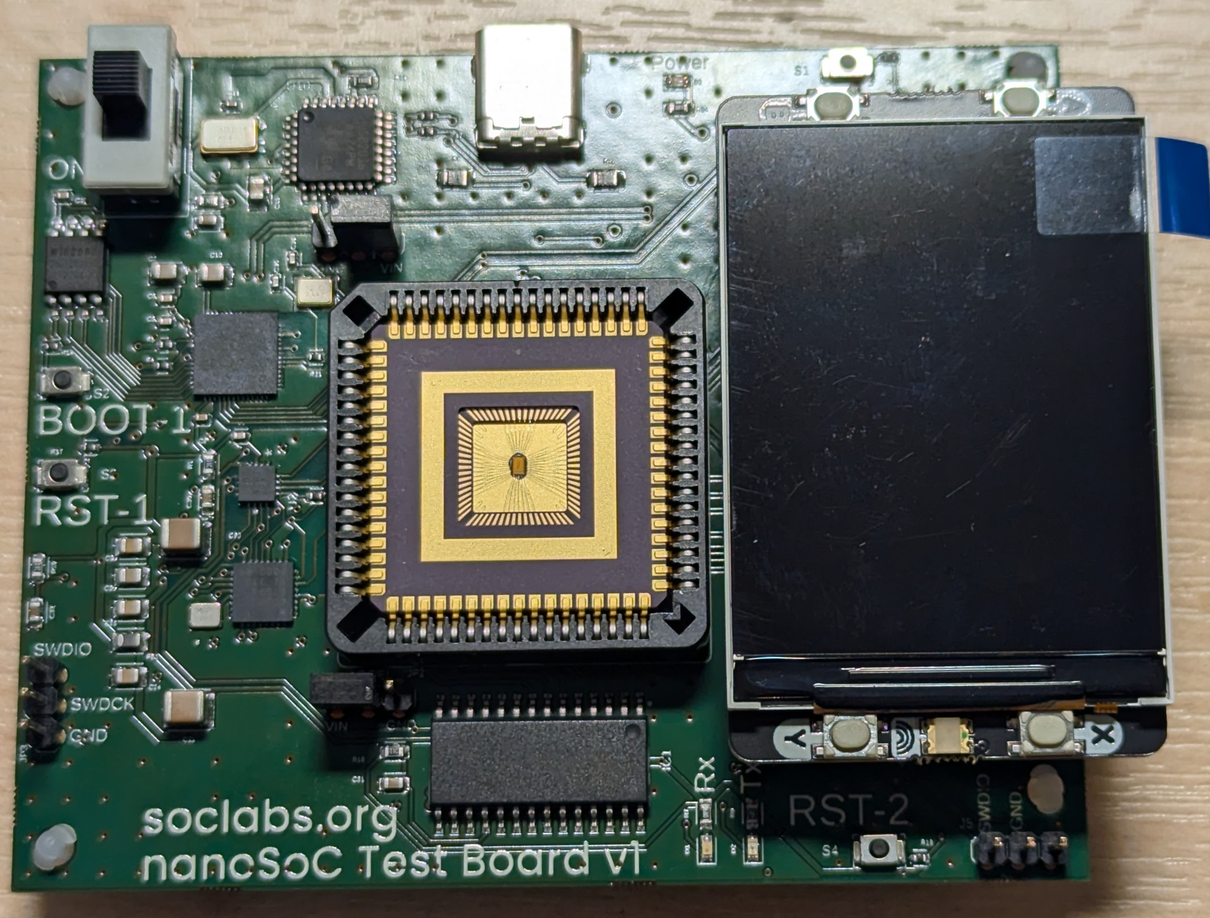
nanoSoC Test/development Board
A physical test environment is required for ASIC devices fabricated following tape out. The nanoSoC test board provides a complete test environment for ASIC designs based on the nanoSoC reference design and enables the showcase of any custom designs that utilise it. Reviewing the function of nanoSoC identifies a number of design criteria for the test board:
- Serial Wire Debug (SWD) and UART debugger interface
- GPIO driver interface including data transport
- Power supply and monitoring
- Clock and reset control
A design choice was made to use the RP2040 chip for all control and monitoring of the nanoSoC ASIC. The RP2040 was chosen for the following reasons: there is a significant amount of support for developing on these chips; the PIO interfaces allow for custom data transfer interfaces which could either be used to implement a FT1248 interface or similar communications; and the RP2040 mirrors well the test bench environment used to develop the nanoSoC hardware (a cortex m0 processor as a debugger). The RP2040 approach allows for a relatively cheap but capable test board.
Based on these requirements, the following test board has been developed:
- A RP2040 SWD and UART debugger
- A RP2040 driver chip with
- SPI Screen
- micro-SD Card
- Power monitoring of VDD and VDDACC power domains
- Clock and reset control
- USB-C interface
The filesystem space in the RP2040 chip can be utilised to download hex/binary test files, test-vectors and expected outputs that can be used to compare ASIC outcomes against defined tests. Another useful feature is an Onscreen display of the current power usage, test progress, and results. The RP2040 debugger can be used to debug code and monitor internal status of the Cortex M0 and nanoSoC system.
Test board sub-systems
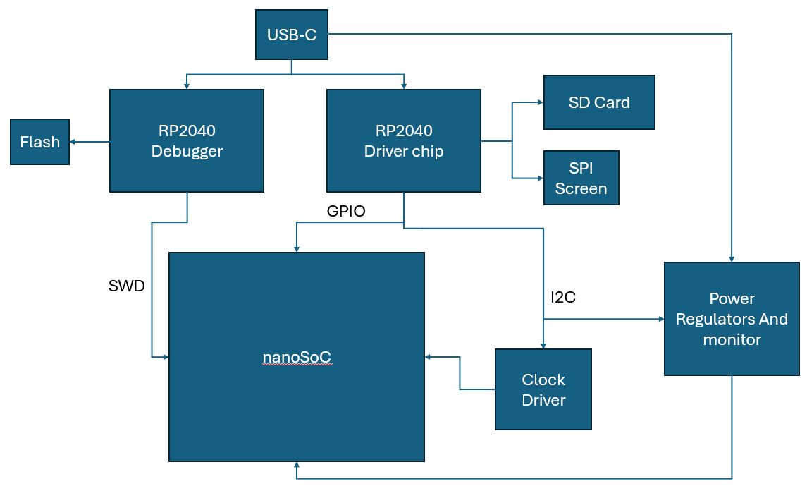
Power regulation and monitoring
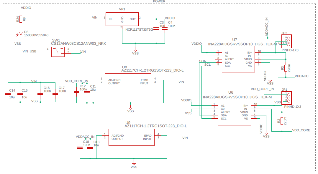
The board comprises of 3 voltage regulators for:
- 3.3V On board power and IO power to nanoSoC
- 1.2V Core power to nanoSoC (VDD)
- 1.2V Accelerator power to nanoSoC (VDDACC)
Power monitoring is achieved using the INA228, a 20-bit precision power monitor with I2C interface. A 220mΩ shunt resistor can monitor currents up to 186mA in high precision mode , or 744 mA in low precision mode with a resolution of 355 nA in high precision or 1.42 µA in low precision mode. There are pin headers for the connection of an external ammeter and voltmeter.
Clock driver
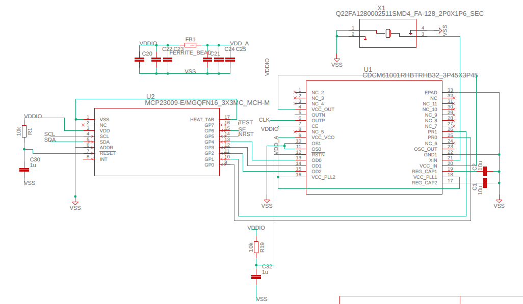
The internal logic of nanoSoC is driven entirely by the external clock requiring a low-jitter clock generator and the CDCM61001 has been chosen. This chip generates a clock up to 625 MHz and has only 27.4 ps total period jitter and 544 fs RMS phase jitter at 250 MHz output. The crystal clock input to this chip is a 12 MHz and the PLL has feedback divider options of 15, 20, 24, 25 and prescaler divider options of 3, 4, and 5. These prescaler and feedback values are driven by the RP2040 driver chip, so it's possible to vary the supplied clock frequency. This can be especially useful for investigating power/energy consumption of custom accelerators vs clock speed. The maximum frequency that the nanoSoC can run off is 240 MHz.
NanoSoC socket
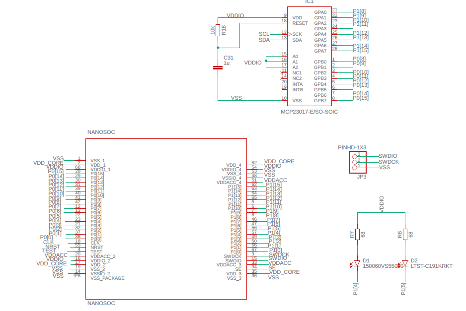
The package chosen for recent nanoSoC tape outs is a JLCC-68 pin package. This can be used with various configuration of GPIOs and the pinout has 38 and 54 pin versions currently. A 68 pin package allows flexibility and reuse of the testboard for different version of nanoSoC ASICs. The GPIO's of nanoSoC are driven primarily from the RP2040 (except for pins P1[4] and P1[5] which are used for UART). To allow for expansion up to 32 IO pins on the nanoSoC, there is also a MCP23017 GPIO expander for the upper 8 pins of each GPIO port (P0[8:15], P1[8:15]).
RP2040 Driver
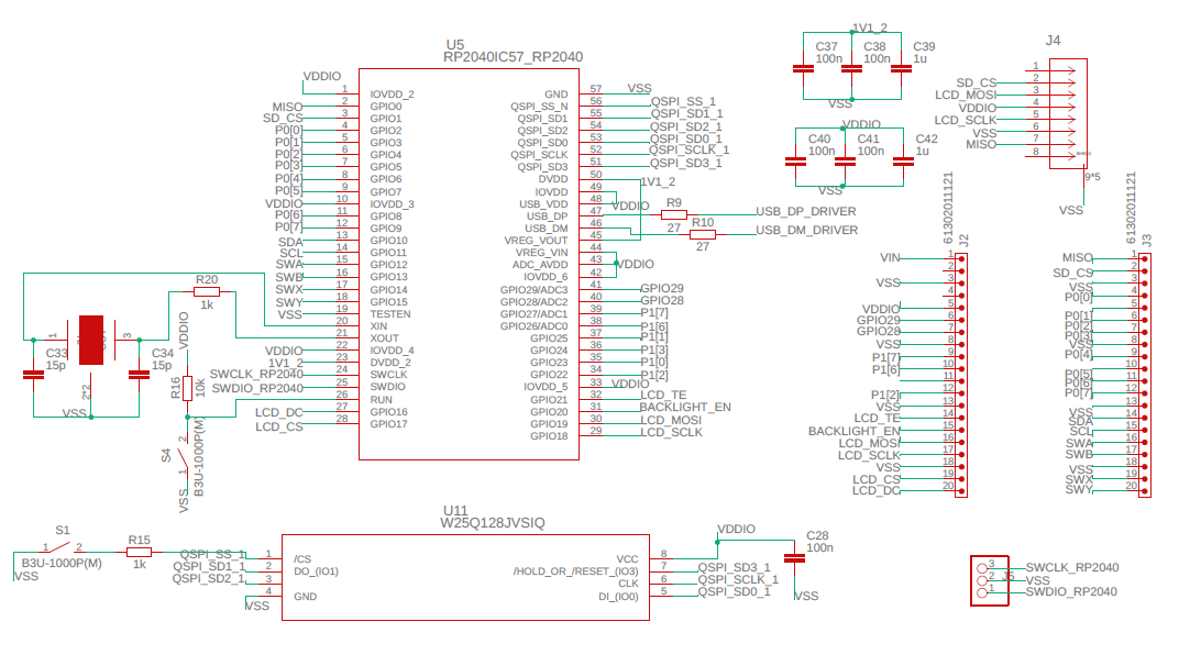
The driver chip has an attached micro-SD card and SPI screen. The screen IO has been configured for a PICO display pack 2.0 which includes some buttons which can be used for the control of the driver program or nanoSoC. The flash chip has a capacity of 16MB, allowing for large applications to run on the RP2040. This enables load of programs/data for the nanoSoC system directly using this flash space as an alternative to the micro-SD card interface.
Prototyping
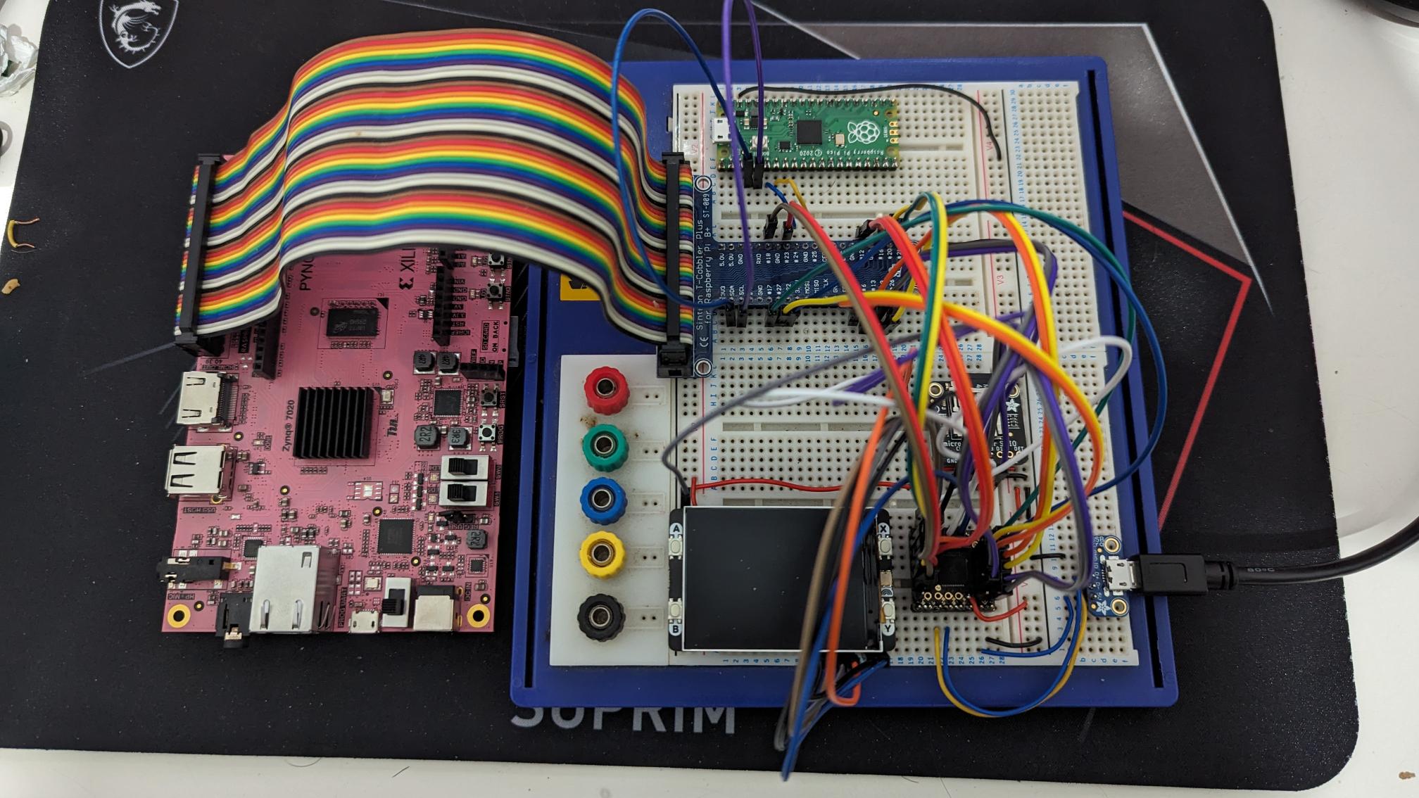
Use of the RP2040 chips in this board design, allowed prototyping using readily available and inexpensive ''evaluation boards'' (i.e. the raspberry pi pico). A prototype of the board could be built before manufacturing the board to ensure verification of core capabilities. This used the Pynq Z2 board to emulate the nanosoc chip with a raspberry pi pico and a PGA2040 (chosen because it gives visibility to all the GPIO pins needed to connect to the nanoSoC) to emulate the final board functions.
Software Development
A software development kit for the nanosoc test board can be found on our git.
The kit contains development material for the software development for the 3 main components of the testboard: nanoSoC, RP2040 debugger and driver. The RP2040 debugger uses the raspberry pi debugprobe code to setup the Serial Wire Debug (SWD) and UART connections. The pins are in the default configurations so no changes are needed. There is also a pre-built .UF2 file that can be directly downloaded to the RP2040 debugger.
NanoSoC software
The nanosoc development kit contains libraries and drivers for:
- DMA 230 and 350
- UART retarget for putc and getc functions
- Cortex-M0 and nanoSoC specific header files
- CMSDK-M0 drivers
Example code projects for the use with Keil uVision (ver. 5 and above). These have been adapted from the nanoSoC test codes and can be copied and adapted for any accelerator application.
RP2040 Driver Software
Includes libraries and drivers for the RP2040, libraries for PIO control for data movement between the RP2040 and nanoSoC, as well as graphics libraries for display on the PICO display 2.0.
Testboard Demo
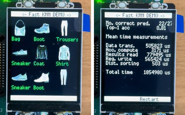
In the nanosoc_board/C_Cxx directory of the repository is a nanosoc_demo project. This can be used as a template demonstrator to "show off" the nanosoc and testboard. This demo drives output to the screen to show a Home screen, Program screen, Console, Demo screen and power screen.
The Program screen can be used to download any programs found in the ./programs directory of the SD card onto the nanosoc chip. The Console screen reads from the nanosoc stdio and displays on the screen. The Demo screen can be used to display visuals of what nanosoc is doing (for instance if you are running image recognition, display the images you are currently processing) . Lastly the Power screen displays the voltage, current and power consumption for the Core power and Accelerator power.
Project Status
The test board is currently under development
Team


Post Silicon Project for:
 Daniel Newbrook
Digital Design Engineer
at University of Southampton
Research area: IoT Devices
ORCID Profile
 Cortex-M0
 Cortex-M0+
![]() Post Silicon
Post Silicon
Submitted on
Comments
Reflect equivalence to the FPGA and simulation test environments
This project needs an update so readers can clearly see how any tests are performed and issues debugged in a consistent way using the test board as for those in the FPGA instantiation and simulation test environments.
Specifically it should cover the method to pass model data through any custom accelerator.
Add new comment
To post a comment on this article, please log in to your account. New users can create an account.