Post Silicon
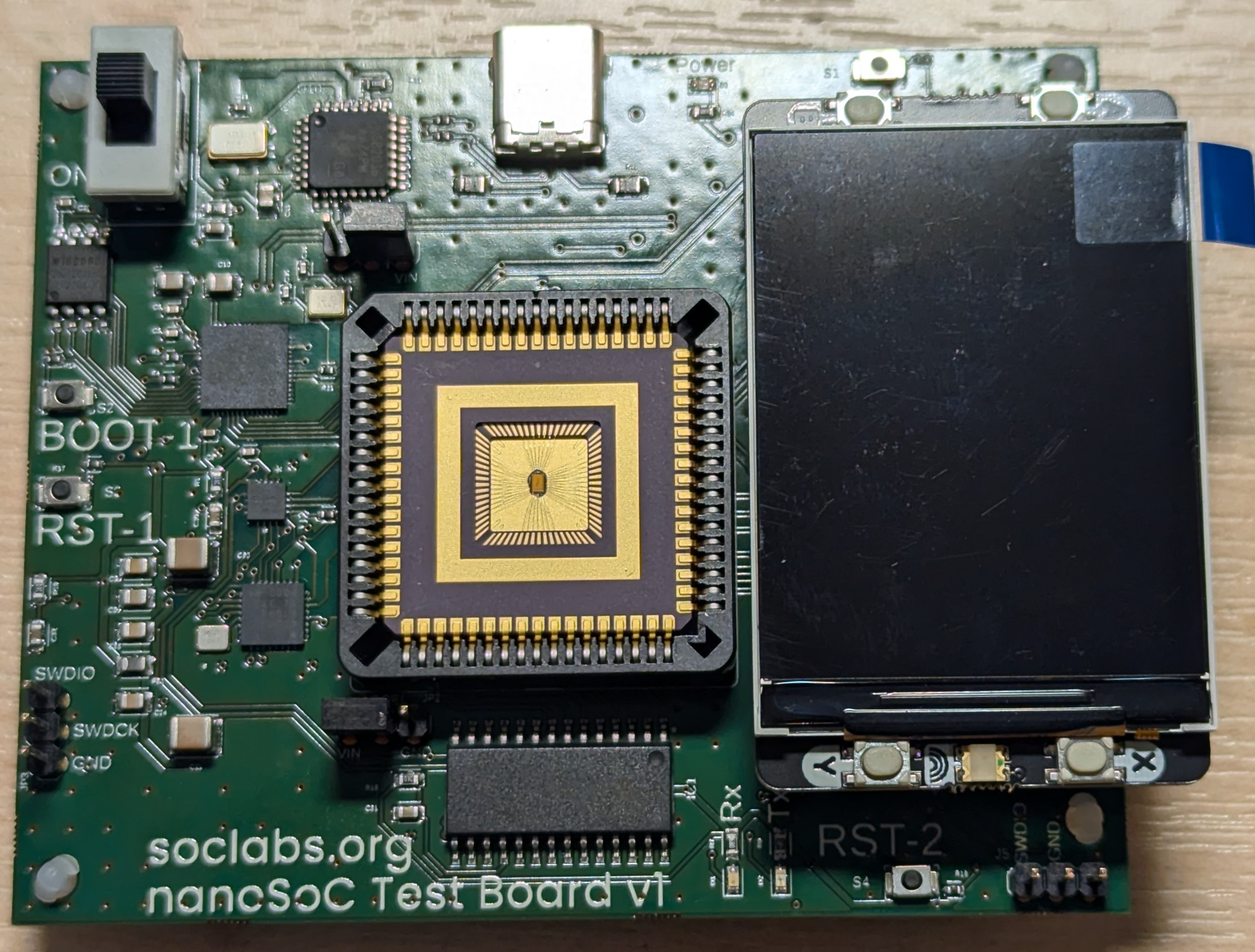
Following the SoC submission to manufacture (tape out) there are an ongoing set of activities in preparation for the return of the fabricated devices. These can include preparation of additional verification assets, the integration of the ASIC into a broader system such a test board or application board, the development of systems software or demonstration applications. Once the silicon devices are returned from manufacturing post silicon validation can begin. Post silicon validation tasks can be quite significant and it is important these tasks are built into the project plans and milestones. As with other aspects of SoC design, the way to manage the effort is to reuse existing pre-qualified silicon validation assets and commonly used tools and environments.
Here are some of the necessary post silicon validation tasks:
Silicon Bring-up
This step involves powering up the device, establishing communication, and ensuring all the major functions of the design are working. It will involve ensuring the device is providing the necessary debug information that might be needed if an error is found. It can involve verify boot checks and other basic functional behaviours before starting the remaining validation tasks are undertaken.
Functional validation
Unfortunately functional failures are a risk especially for first-time designs and academic teams who too often do not develop and execute a full range of pre-manufacture verification tasks. Functional validation operates the design with various tests and software to validate the SoC and ensure it works to the expected operating conditions. The validation my be undertaken sub-system by sub-system, exercising the various IP blocks, for example, the memory subsystems of an SoC are tested both with random test patterns and the real world data for normal operation. Issues in memory subsystems can have significant impact on any SoC. Some validation tests are software tests run on the CPU within the SoC itself. Some of the tests come from the external environment, such as a test board, that generate signals or pass data into the system with the external connections acting as an observer of expected results. Validation plans should cover various system configurations, features to be verified, and use scenarios that need confirming.
Performance validation
The performance of the fabricated device may well vary from the performance estimated during the pre-fabrication simulations stages. The actual performance of core system IP as well as communications interfaces must validated for speed and performance by driving their respective interfaces. In an academic setting system performance can be determined in many ways and comparisons to other research outcomes an important consideration.
Power validation
In normal post silicon validation these activities validate the power management flows within the device and analyze the systems power consumption. In an academic setting projects are often concerned with establishing the energy efficiency of a newly researched design concept. Ensuring accurate recording of energy consumption from the various power domains in the SoC is an important aspect of the post silicon validation process. The task may involve adjusting the system performance to vary how much power is consumed for a variety of work load and system stress.
The nanoSoC test board allows power monitoring of VDD and VDDACC power domains to obtain energy use separately for the SoC and any specific custom accelerator core.
Post silicon debug
The debug architecture of the specific SOC reference design varies.
For nanoSoC the debug architecture is based on the basic arm cortex M0. Due to the requirement for limited area fault status registers are not available in the M0 and identifying hard fault issues is more time consuming. The nanoSoC test board uses a Raspberry Pi RP2040 device to provide the Serial Wire Debug (SWD) and UART debugger interface.
In an academic project it may not be necessary to engage in all the post silicon validation that a commercial product requires.
- An exhaustive test plan for every IP component in the SoC design.
- Repeated testing of multiple silicon devices to characterize the process variations.
Explore This Design Flow
Projects Using This Design Flow

Experts and Interested People
Members
Related Project Milestones
| Project | Name | Target Date | Completed Date | Description |
|---|---|---|---|---|
| Aspen: A 630 FPS Real-Time Posit-Based Unified Accelerator for Extended Reality Perception Workloads | Post Silicon (191) | |||
| RF-Powered Sensor Platform for Intelligent Groceries Transportation Monitoring | Post Silicon (191) |
Designed and fabricated the test PCB to test the chip. |


Add new comment
To post a comment on this article, please log in to your account. New users can create an account.