
Hell Fire SoC
Systolic arrays are critical in parallel computing. They efficiently accomplish tasks like matrix multiplication and signal processing by coordinating a grid of processing components to perform synchronized operations. The structured data flow reduces memory access while increasing processing, resulting in substantial speedups. Systolic arrays are used in a variety of domains, from AI model training to scientific simulations, to improve speed and enable complicated computations that typical sequential approaches struggle with. Their importance in increasing computing capabilities across multiple fields is highlighted by their role in expediting activities while maximizing resource efficiency.
Project Milestones
Do you want to view information on how to complete the work stage ""
or update the work stage for this project?
-
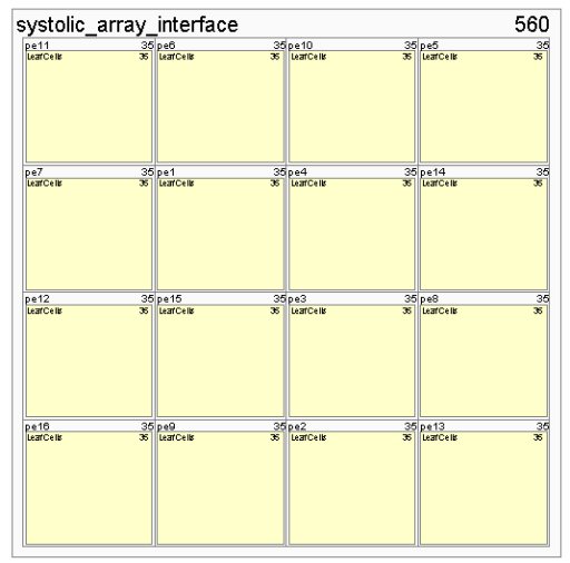
Systolic Array Design
Target DateCompleted DateWe developed a Processing Element (PE) comprising an accumulator and a multiplier for the Systolic Array implementation within our SoC. To ensure the IP's readiness for successive cycles of operations and avoid a global reset, we adopted a separate reset mechanism for the accumulator. This approach enhances the efficiency of the Systolic Array, allowing for seamless and independent reset of individual PEs during each cycle of computation. The use of separate resets minimizes overhead and contributes to improved performance and scalability of the overall system.
-
Accelerator IP Interface
Target DateCompleted DateWe opted for 32-bit wide Non-Sequential transfers to provide continuous data delivery to the Array Interface IP. This purposeful approach provides efficient data transmission while also simplifying the overall architecture. We achieve exact data transfer throughout the system by applying appropriate control signals. This method helps to a more streamlined and ordered data flow, which improves the functionality of the Array IP. The usage of 32-bit data width, together with diligent control signal management, ensures accurate and timely data transmission, eventually improving system performance.
-
AHB Memory Interface Design
Target DateCompleted DateThis Interface implements a byte-addressable memory interface assuming a 32-bit memory width.
-
AHB GPIO Interface
Target DateCompleted DateAHB Based GPIO Interface
-
Array Alignment Interface
Target DateCompleted DateAs the data to the array has to be aligned we plan to implement a data storage, alignment, and delivery architecture that accepts the data via the incoming AHB-Lite transfers and performs the operation and delivers the results back to the memory via the memory interface.


-
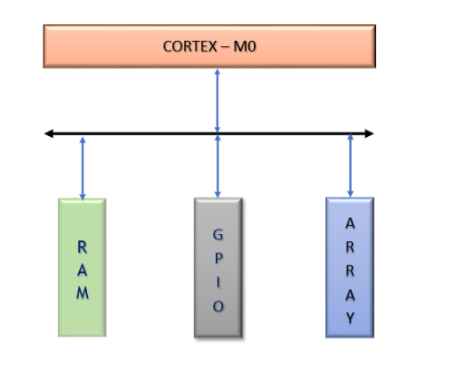
SoC Intergration
Target DateThe Systolic Array, GPIO, and memory peripherals are integrated to the Cortex-M0 and the SoC is tested.
-
Physical Implementation
Target DateCompleted DateThe Array IP was implemented on TSMC 65nm using Cadence Genus and Innovus tools. The table provided below offers insights into the diverse implementation runs conducted during the design phase, highlighting the evolution and refinement process of the Array IP. These iterative runs allowed us to fine-tune the IP's performance, power efficiency, and area utilization, ensuring that the final implementation met stringent design specifications.
Block Implementation Report Period(ns) Frequency(MHz) Area(um2) Power(mW) PPA(mW/um2) 1.33 751.88 37662.48 38.72 1.03e-3 2.0 500 31237.56 18.78 6.01e-4 4.0 250 30402.36 8.49 2.79e-4 10.0 100 30020.04 3.29 1.09e-4 -
Tape Out
Design FlowTarget DateCompleted DateSubmit for tapeout to europractice TSMC 65nm mini ASIC shuttle

Team


 Project Creator
 Srimanth Tenneti
Researcher
at University of Cincinnati
Research area: Machine Learning | SoC Design
![]() Software
Software
Submitted on
Comments
Project Update
Hello Everyone,
I’m excited to share some significant improvements we’ve made to the IP. We’ve successfully reduced latency from 96 cycles to just 25 cycles while introducing advanced features like 2x writes before read and support for IS, WS, and OS data flows—all without significantly increasing the area of these units.
Additionally, we’ve integrated a Gen-1 matrix transpose block and an activation block into the IP, enhancing its power and capabilities. These upgrades mark a major leap forward in performance and functionality.
While the release is still a work in progress, with more updates on the way, we’re thrilled about what’s coming. Stay tuned for further developments.
Thanks and regards,
Srimanth Tenneti
Final demonstration and additional information on the project
Hi,
It would be great to get an update on the final demonstration of the accelerator working on the test board and also an update to the project to reflect on the start to finish milestones and any reflections on the lessons learned along the way.
We look forward to hearing about your thoughts on this.
Die are back
Srimanth,
The die are back. Are you ready for testing the design with the test board?
John.
Collaboration
Hello Everyone,
Our goal with this project was to introduce an Open Accelerator platform, and now, we're eager to invite all of you to join us in taking it to the next level.
We value your input, creativity, and collaboration. Together, we can enhance this design in countless ways. Your engagement and suggestions are not only welcomed but crucial to our success.
Thank you for being a part of this journey, and we look forward to your valuable contributions.
Warm Regards,
Srimanth Tenneti
GitHub - https://github.com/srimanthtenneti/Hell_Fire_SoC_Demo/
Update1
Update1
Accelerator Interface
Hi Sri,
I hope your project is going well. What is your plan for your accelerator interface? Are you planning on building an AHB-Lite based interface directly into your accelerator or are you planning on building/using a wrapper level to translate your transactions?
Thanks,
David
Hi David, I plan to use a…
Hi David,
I plan to use a direct interface.
Thanks, & Regards
Srimanth Tenneti
Use of the DMA and NanoSoC reference design
Thanks for the project outline. Hopefully you are well into the Design of a 5x5 systolic array with input alignment. From that and looking at the data requirements you may be able to see how David Mapstone uses the DMA in the NanoSoC reference design to push/pull data from the accelerator. Your wrapper interface is going to differ from his implementation but hopefully it will act as a starting point. If you need any help then please let us know.
We also hope the item on how to structure a Project and our example projects help you get set up quickly for this project.
Structure for the Project
Hopefully we have a clear pathway now to establish the Project and set up the repositories. If I understand things this Project will use the the NanoSoC reference design to push/pull data from the accelerator.
na
na
Add new comment
To post a comment on this article, please log in to your account. New users can create an account.