NanoSoC Ethernet Subsystem
Introduction
Embedded systems that require deterministic, low-latency Ethernet connectivity face an architectural design choice. One option is using the main SoC processor to share its execution time between application logic and network protocol handling. Even with lightweight TCP/IP stacks, the overhead of frame reception, protocol parsing, buffer management, and retransmission can consume significant CPU cycles. This is particularly the case in small Microcontroller SoC systems where the main processor is likely resource-constrained.
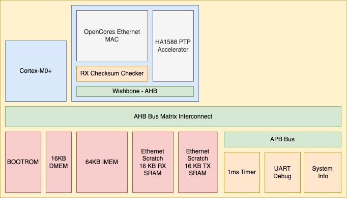
The NanoSoC Ethernet Subsystem addresses this by packaging a complete TCP/IP offload engine into a reusable, self-contained AHB subsystem. The subsystem contains a dedicated ARM Cortex-M0 processor for network protocol handling combined with an OpenCores Ethernet MAC, IEEE 1588 PTP hardware timestamping, and dedicated local memories. The subsystem runs its own firmware stack (picoTCP) and communicates with the rest of the SoC through standard AHB bus interfaces. The host system sees it as a peripheral with simple mailbox-style communication avoiding the complexity of host; shared-memory coordination, interrupt storms and other driver related handling.
Context
The next generation of NanoSoC provides a modular, YAML-driven SoC generation framework where subsystems are defined declaratively and assembled into complete chip designs. Each subsystem exposes standard AHB slave and master ports, allowing the top-level interconnect generator to wire them into the address map automatically.
The NanoSoC Ethernet Subsystem is being designed to fit this model: a drop-in block that provides Ethernet connectivity to any NanoSoC based design. The subsystem handles everything from PHY-level frame I/O through to TCP socket management, presenting a simple register or shared-memory interface to the host.
Key design constraints:
- Bus protocol: AHB-Lite (consistent with the NanoSoC ecosystem)
- Technology: TSMC 65nm LP (tape-out target), Xilinx Zynq (FPGA prototyping)
- Area budget: < 1 mm^2 including memories
- Clock target: 250 MHz (ASIC), 25 MHz (FPGA), (consistent with the NanoSoC ecosystem)
- IP reuse: Leverage open-source Ethernet MAC and PTP cores where possible
The Solution
The subsystem offers complete Ethernet connectivity with a dedicated microcontroller.
The Cortex-M0 boots from ROM, loads firmware into IMEM via the bootloader's remap mechanism, and then runs picoTCP. The Ethernet MAC's DMA engine moves frames between the MII PHY interface and the scratch SRAMs. The CPU processes frames through the TCP/IP stack, while the HA1588 PTP core provides hardware-assisted timestamping for IEEE 1588 time synchronisation.
Subsystem Architecture
Memory Map
| Address | Size | Target | Description |
|---|---|---|---|
0x00000000 | 128 MB | Boot ROM / IMEM | Boot ROM at reset; remaps to IMEM after boot |
0x08000000 | 128 MB | Boot ROM | Boot ROM (direct access, always mapped) |
0x10000000 | 128 MB | IMEM | Instruction memory (64 KB physical) |
0x18000000 | 128 MB | DMEM | Data memory (16 KB physical) |
0x20000000 | 256 MB | System | Passthrough to external AHB master port |
0x30000000 | 128 MB | Scratch RX | Ethernet receive frame buffers (16 KB) |
0x38000000 | 128 MB | Scratch TX | Ethernet transmit frame buffers (16 KB) |
0x40000000 | 128 MB | Ethernet MAC | MAC registers (0x0000) + PTP registers (0x1000) |
0x50000000 | 256 MB | APB Peripherals | Timer, UART, system controller |
Interconnect
The internal bus matrix is a 4-initiator x 8-target AHB-Lite crossbar:
Initiators:
- CPU --- full access to all 8 targets
- Ethernet MAC DMA --- access to scratch SRAMs, IMEM, DMEM, and the system passthrough
- External slave port 0 --- host system access to subsystem resources
- External slave port 1 --- second host access port (independent arbitration)
System passthrough: CPU addresses above 0x20000000 that don't hit a local target are forwarded out through the AHB master port, allowing the subsystem's firmware to access host system memory or peripherals directly.
Components
ARM Cortex-M0 Processor
The subsystem uses a core Cortex-M0 processor (not the integration-level wrapper) with debug (SWD), SysTick timer, WIC (wake-up interrupt controller), 32 IRQ lines, and 4 breakpoint comparators. A lightweight Power and Reset Management Unit (PRMU) generates HCLK and HRESETn from the free-running input clock, providing clean reset sequencing.
At approximately 53,000 um^2 in TSMC 65nm, the M0 represents about 20% of the logic area --- a modest cost for a dedicated protocol processor.
OpenCores Ethernet MAC
The OpenCores Ethernet MAC (eth_top) is an IEEE 802.3 10/100 Mbps MAC by Igor Mohor with a Wishbone bus interface, MII PHY connection, and a DMA engine that manages frame transmission and reception through buffer descriptors stored in an internal 8 KB SRAM.
The original Wishbone interface is bridged to AHB-Lite using a pair of protocol bridges:
ahb3lite_to_wb--- converts AHB slave transactions to Wishbone for register accesswb_to_ahb3lite--- converts the MAC's Wishbone DMA master to an AHB master for frame buffer access
Patches applied to the OpenCores MAC:
- SystemVerilog keyword fix (
eth_spram_256x32.v): Renamed thedooutput port todo_o. The original name is a reserved keyword in SystemVerilog (do...while), causing compilation failures with-sverilogmode required by cocotb and modern synthesis tools. - SRAM wrapper abstraction (
eth_spram_256x32.v): Replaced the original compile-timeifdefblock (which selected between generic, Xilinx, Artisan, and Virtual Silicon SRAM implementations) with a cleanethmac_sramwrapper module. Three variants are provided and selected via filelist:fpga/ethmac_sram.v--- wraps ARM CMSDKcmsdk_fpga_sramfor FPGAgeneric/ethmac_sram.v--- register-based for simulationasic/ethmac_sram.v--- compiled SRAM macro for ASIC
- BIST removal (
eth_wishbone.v): Stripped the Built-In Self-Test port connections from the buffer descriptor RAM instantiation to match the simplified SRAM wrapper interface.
OpenCores HA1588 IEEE 1588 PTP Core
The OpenCores HA1588 (ha1588) is a hardware-assisted IEEE 1588-2008 Precision Time Protocol core by BABY&HW. It provides:
- Real-Time Clock (RTC): 48-bit seconds + 32-bit nanoseconds + sub-nanosecond fractional accumulator with 2^-32 ns period resolution. Supports direct time write and frequency adjustment.
- Time Stamping Unit (TSU): Line-speed PTP packet detection on GMII, configurable 8-bit event message type mask, and a 15-entry timestamp queue (128 bits: 16-bit metadata + 80-bit timestamp + 32-bit packet ID).
The HA1588 monitors the MII interface passively --- it taps the same TX/RX data lines that connect the MAC to the PHY, capturing timestamps at the point where frames cross the wire. Since the subsystem uses MII (4-bit) rather than GMII (8-bit), the 4-bit data is zero-padded to 8 bits and giga_mode is tied low.
Patches applied to HA1588:
- Reset hygiene (
ha1588.v): The original design only had a software-controlledrtc_rstfor the RTC and queue modules --- system reset (rst) was not propagated, leaving the RTC and timestamp FIFOs uninitialised on power-on. The patch adds a 2-FF reset synchroniser into thertc_clkdomain and OR-gates system reset with the software reset for all sub-modules. This is critical for deterministic ASIC reset sequencing. - Register reset (
reg.v): All internal registers in the register module (data output, time capture, queue status, CDC synchroniser flip-flops) now have proper synchronous reset. The original had no resets, causing X-state propagation in simulation and undefined power-on state in silicon. - RTC self-assignment fix (
rtc.v): Fixed two reset clauses whereperiod_fix <= period_fixandtime_adj <= time_adj(self-assignments that prevent initialisation) were changed to zero assignments. - Generic async FIFO (
ptp_queue.v): Completely replaced the vendor-specific FIFO implementations (selected viaUSE_ALTERA_IP/USE_XILINX_IPmacros) with a portable dual-clock asynchronous FIFO using gray-code pointer synchronisation. 128-bit data width, 16-entry depth. This eliminates vendor lock-in and works across simulation, FPGA, and ASIC flows.
Interfaces
External Bus Ports
| Port | Type | Direction | Width | Description |
|---|---|---|---|---|
cpu_0 | AHB-Lite | Master out | 32/32 | System passthrough (CPU traffic to host) |
eth_ss_0 | AHB-Lite | Slave in | 32/32 | Host access port 0 |
eth_ss_1 | AHB-Lite | Slave in | 32/32 | Host access port 1 |
Ethernet PHY Interface (MII)
| Signal | Direction | Width | Description |
|---|---|---|---|
mtx_clk_i | In | 1 | Transmit clock (25 MHz @ 100 Mbps) |
mtxd_o | Out | 4 | Transmit data |
mtxen_o | Out | 1 | Transmit enable |
mtxerr_o | Out | 1 | Transmit error |
mrx_clk_i | In | 1 | Receive clock (25 MHz @ 100 Mbps) |
mrxd_i | In | 4 | Receive data |
mrxdv_i | In | 1 | Receive data valid |
mrxerr_i | In | 1 | Receive error |
mcoll_i | In | 1 | Collision detect |
mcrs_i | In | 1 | Carrier sense |
md_pad_i/o | Bidir | 1 | MDIO management data |
mdc_pad_o | Out | 1 | MDIO management clock |
PTP Time Outputs
| Signal | Width | Description |
|---|---|---|
rtc_time_ptp_ns | 32 | PTP nanoseconds |
rtc_time_ptp_sec | 48 | PTP seconds |
rtc_time_one_pps | 1 | One pulse-per-second |
Debug and Control
| Signal | Direction | Description |
|---|---|---|
uart_rxd/txd | In/Out | Debug UART (38400 baud) |
cpu_0_swd | Bidir | Serial Wire Debug |
eth_irq | Out | Ethernet MAC interrupt |
cpu_0_irq[31:0] | In | External interrupt inputs |
Firmware Stack
Architecture
The subsystem runs a bare-metal firmware stack built on picoTCP, a lightweight, modular TCP/IP library designed for embedded systems:
  +-----------------------------------------------+
  |              Application Layer                 |
  |  (UDP echo server, telnet, custom protocols)   |
  +-----------------------------------------------+
  |               picoTCP Stack                    |
  |  TCP | UDP | ICMP | ARP | IPv4 | CRC           |
  |  (~38 KB .text with IPv6 disabled)             |
  +-----------------------------------------------+
  |          MAC Driver (eth_ss_picotcp_port.c)    |
  |  TX: 4 buffer descriptors, scratch TX SRAM     |
  |  RX: 8 buffer descriptors, scratch RX SRAM     |
  |  Frame size: 1536 bytes, 32-byte aligned       |
  +-----------------------------------------------+
  |          Hardware Abstraction                  |
  |  Register access | Timer ticks | UART debug    |
  +-----------------------------------------------+
Boot Sequence
- CPU fetches reset vector from Boot ROM at
0x00000000 - Bootloader initialises the debug UART (38400 baud, 25 MHz clock)
- Prints
"EthSS Boot"banner - Writes
REMAP=1to the system controller register at0x50002000 - Branches to
0x00000000--- now mapped to IMEM - CPU reloads MSP and PC from the firmware's vector table in IMEM
- Firmware initialises picoTCP, configures the MAC, and enters its main loop
MAC Driver
The MAC driver (eth_ss_picotcp_port.c) manages the OpenCores Ethernet MAC's buffer descriptor ring:
- TX path: 4 descriptors pointing into scratch TX SRAM (
0x38000000). Frames are copied from picoTCP's buffer chain, descriptors are configured with PAD, CRC, and IRQ flags, and the MAC's DMA engine transmits via MII. - RX path: 8 descriptors pointing into scratch RX SRAM (
0x30000000). The MAC DMA writes received frames, the driver polls descriptor status, copies frames into picoTCP buffers, and recycles descriptors. - Frame size: 1536 bytes maximum, 32-byte aligned for DMA efficiency.
Timer Integration
A 1 ms APB timer (CMSDK cmsdk_apb_timer, 25 MHz / 25,000 divider) provides millisecond ticks for picoTCP housekeeping --- ARP cache expiry, TCP retransmission, keepalive timers, and socket timeouts.
Integration into a Host SoC
Bus Connections
The subsystem presents three AHB-Lite ports to the host system:
- Master out (
cpu_0): The subsystem's CM0 can access host memory and peripherals at addresses >=0x20000000. This enables the subsystem firmware to read/write shared memory regions, signal the host via doorbell registers, or access host-side peripherals directly. - Slave in (
eth_ss_0,eth_ss_1): The host processor can access the subsystem's memories, MAC registers, and PTP clock. Typical host operations include preloading firmware into IMEM, reading PTP timestamps, configuring the MAC, or inspecting packet buffers.
Clock Domains
The subsystem has four clock domains:
| Domain | Source | Frequency | Drives |
|---|---|---|---|
sys_fclk | External | 25--250 MHz | CM0, AHB interconnect, memories, APB |
rtc_clk | External | 25--250 MHz | HA1588 RTC (PTP timebase) |
mtx_clk | PHY | 2.5/25 MHz | MII transmit path |
mrx_clk | PHY | 2.5/25 MHz | MII receive path |
CDC crossings between these domains are handled by the OpenCores MAC (TX/RX FIFO synchronisers) and the HA1588 PTP core (gray-coded async FIFOs in the timestamp queues, reset synchronisers in the RTC).
IEEE 1588 Precision Time Protocol
Why Hardware Timestamping Matters
Software only PTP implementations timestamp frames in the driver or stack. This can introduce jitter from interrupt latency, context switches, and bus contention. Hardware timestamp capture at the MII interface, as close to the wire as possible, eliminating software jitter and enabling sub-microsecond synchronisation accuracy.
How It Works in This Subsystem
The HA1588 PTP core monitors the MII TX and RX data lines passively. Its Time Stamping Unit (TSU) performs line-speed PTP packet detection by parsing Ethernet frames as they flow through the interface:
- The TSU watches for PTP EtherType (
0x88F7) in the Ethernet header - On detection, it snapshots the current RTC time into its timestamp queue
- The queue stores 128-bit entries: 80-bit timestamp + 32-bit sequence ID + 16-bit metadata
- Firmware reads the queue via the PTP register interface to correlate timestamps with PTP messages
A separate PTP event detector (ptp_event_detector.v) provides a lightweight, independent frame detection mechanism. It monitors MII nibbles, detects SFD, counts through the MAC header (12 bytes), and checks for EtherType 0x88F7, producing a single-cycle pulse on match. Toggle-based CDC synchronisers safely transfer these pulses from the MII clock domains to the system clock domain.
RTC Time Outputs
The RTC's current time (rtc_time_ptp_ns, rtc_time_ptp_sec, rtc_time_one_pps) is exported as top-level outputs, enabling system-wide time distribution. Other SoC based subsystems can then synchronise their local clocks to this reference.
Data Movement
Frame Transmission
  Application     picoTCP        MAC Driver           Hardware
  ───────────     ────────       ──────────           ────────
  send(data)
       │
       └──> pico_socket_send()
                  │
                  └──> TCP/UDP encapsulation
                       IP header, checksum
                       ARP resolution
                            │
                            └──> eth_send()
                                    │
                                    ├── Copy frame to Scratch TX SRAM
                                    │   (CPU write via AHB to 0x38000000)
                                    │
                                    ├── Configure buffer descriptor:
                                    │   pointer, length, PAD, CRC, IRQ
                                    │
                                    └── Set descriptor READY bit
                                            │
                                            └──> MAC DMA reads descriptor
                                                 MAC DMA reads frame from
                                                 Scratch TX via AHB master
                                                 MAC serialises to MII TX
                                                 HA1588 TSU timestamps TX
Frame Reception
  Hardware               MAC Driver           picoTCP            Application
  ────────              ──────────           ────────           ───────────
  PHY receives frame
  MAC deserialises MII RX
  HA1588 TSU timestamps RX
  MAC DMA writes frame to
  Scratch RX (0x30000000)
  MAC sets descriptor DONE
       │
       └───────────> Driver polls descriptors
                     Reads frame from Scratch RX
                       (CPU read via AHB)
                          │
                          └─────────────> pico_stack_recv()
                                          ARP / IP / TCP / UDP
                                          demultiplexing
                                               │
                                               └──────────────> Socket callback
                                                                Application receives data
DMA and Bus Traffic
The Ethernet MAC DMA engine is an independent AHB master on the bus matrix. It accesses the scratch SRAMs, IMEM, and DMEM without CPU intervention. The bus matrix arbitrates between the CPU, MAC DMA, and the two external slave ports, ensuring that DMA transfers don't stall the CPU unless they contend for the same target simultaneously.
Dedicated scratch SRAMs for RX and TX eliminate contention between DMA frame transfers and CPU instruction/data fetches --- the most common source of performance degradation in shared-memory Ethernet designs.
ASIC Area
Synthesised for TSMC 65nm LP at 250 MHz (Synopsys Design Compiler U-2022.12):
| Block | Area (um^2) | % |
|---|---|---|
| Ethernet MAC + PTP subsystem | 192,783 | 21.0% |
| Cortex-M0 core | 53,431 | 5.8% |
| AHB interconnect (4x8) | 14,770 | 1.6% |
| APB peripherals | 5,276 | 0.6% |
| Boot ROM (logic) | 3,042 | 0.3% |
| Logic subtotal | 269,308 | 29.3% |
| SRAM macros (7 instances, 128 KB total) | 696,907 | 70.7% |
| Total | ~918,000 | ~0.92 mm^2 |
The design meets timing at 250 MHz with zero setup violations. Hold violations (40, all on SRAM macro pins) are expected pre-CTS and will be resolved during place-and-route.
Verification
Cocotb Integration Tests
The subsystem is verified end-to-end using cocotb (Python) with VCS as the simulator. The testbench drives the MII interface with Ethernet frame models and monitors the UART debug output:
test_bootrom_uart_banner--- verifies the boot ROM executes and prints the expected banner on the debug UART after resettest_firmware_preload_and_run--- preloads firmware into IMEM, boots, and verifies the application starts successfullytest_arp_response--- sends an ARP request to the DUT's IP address and verifies a correct ARP reply with the configured MAC addresstest_udp_echo--- full end-to-end test: ARP resolution, UDP echo request, and verification of the echoed payload (RFC 862)test_socket_echo--- TCP socket-level echo test
Component-Level Verification
The ethernet-mac-ahb submodule has its own extensive test suite:
- Bridge tests:
ahb3lite_to_wb,wb_to_ahb3lite,rmii_to_mii - MAC tests:
ethmac_ahb, C-driver-in-the-loop, echo loopback - PTP tests:
ha1588_ahb,ptp_event_detector, servo synchronisation - UVM tests: Formal verification of bridges, HA1588, and full subsystem
- CDC analysis: Synopsys SpyGlass on
ethmac_subsystem_apb(4 clock domains) andethmac_ahb(3 clock domains)
CI Pipeline
The GitLab CI pipeline runs:
- Setup --- clone, submodule init, preflight tool/IP validation
- Generate ---
soc_modelgeneration (interconnect, top-level SV, firmware configs) - Lint --- HAL structural lint + SpyGlass CDC analysis
- Test --- cocotb boot and UDP echo tests
- Synthesis --- RTL Architect (area/timing exploration) + Design Compiler (gate-level netlist) + Vivado FPGA synthesis (Pynq-Z2)
Future Work
Cortex-M0+ Upgrade
The current Cortex-M0 core could be replaced with a Cortex-M0+ for marginal area cost. The M0+ adds a 2-stage pipeline (vs 3-stage in M0), reducing branch penalty and power, and provides the Micro Trace Buffer (MTB) for non-intrusive firmware debug. The slcorem0 wrapper in nanosoc_arch_tech already abstracts the core interface, making this a configuration change rather than an architectural one.
IMEM Sizing and Structure
The 64 KB IMEM configuration fits picoTCP with IPv4, UDP, TCP, and basic application logic, but leaves little room for growth. Two approaches are being considered:
- Overlay architecture: A 3-bank IMEM with ping-pong firmware loading, allowing the host to update firmware segments while the subsystem continues executing from the active bank. This is documented in
docs/imem_overlay_architecture.md. - IMEM reduction: Profiling the picoTCP build to identify unused protocol modules and reduce .text below 32 KB, freeing SRAM area for other uses.
QSPI Flash Boot
Currently, firmware is preloaded into IMEM by the host system via the AHB slave port or by the cocotb testbench. A QSPI flash controller (connected via the system passthrough or as a local APB peripheral) would enable autonomous boot from external flash, eliminating the host dependency during power-on. The bootloader would be extended to read firmware from QSPI into IMEM before remapping.
Inline Checksum Accelerator
TCP and UDP checksum computation is a significant CPU overhead in the picoTCP stack, particularly for large frames. A hardware checksum accelerator placed inline between the Ethernet MAC and the AHB-to-Wishbone bridge could compute the one's-complement checksum as frames flow through the DMA path, offloading the CPU entirely. The accelerator would:
- Monitor Wishbone transactions between the MAC DMA and the bus bridge
- Accumulate the running checksum as frame data passes through
- Expose the computed checksum via a register that firmware reads after frame reception (RX offload) or writes before transmission (TX offload)
This is architecturally similar to the TCP Segmentation Offload (TSO) and checksum offload features found in high-performance NICs, scaled down to the Wishbone/AHB subsystem level.
 David Mapstone
SoC Labs Team at University of Southampton
 Cortex-M0
Submitted on
Comments
Behavioural Design milestone
Can you add your Behavioural Design milestone.
John.
QSPI Flash Boot option
Given an academic research perspective what are the architectural design consideration trade offs for this independent QSPI Flash Boot option.
What is the independence buying and what is it costing.
In an academic research I am not sure we are concerned with time to boot. In terms of measuring some part of system performance in order to determine research findings what is being gained from 'eliminating the host dependency during power-on'. For example is power saving during power-on a real concern.
It would be nice to see a clear articulation of the needs, benefits and costs.
John.
Stack rank the Future Work
I raise the points above as a good example of design considerations that go into any Architectural Design phase. We have a set of enhancements that could be made but how do we rank them in order to decide which is the best to apply community resources towards.
John.
Clarification on the M0 integration
Hi,
You mention that "The subsystem uses a core Cortex-M0 processor (not the integration-level wrapper) ...."
What did you mean by 'not the integration-level wrapper'?
Hopefully this is obvious but I just wanted to make sure what was meant.
John.
Add new comment
To post a comment on this article, please log in to your account. New users can create an account.