




AHB eXcecute in Place (XiP) QSPI
The instruction memory in the first tape out of nanosoc was implemented using SRAM. The benefit was the read bandwidth from this memory was very fast, the downside was on a power-on-reset, all the code was erased as SRAM is volatile memory. An alternative use of non-volatile memory would benefit applications where deployment of the ASIC does not allow, or simply time is not available for programming the SRAM after every power up.
Non-volatile memory ("NVM") comes in different forms, but for microcontrollers the most typical type of NVM is flash. In industrial scale tape outs, companies may opt for on chip flash, as the area cost of adding this is typically recovered in selling large volumes of chips. For academic tape outs, the area needed for flash can be costly. The alternative is off-chip flash. There are really 2 categories, parallel and serial. As expected, parallel flash can give higher bandwidth at the cost of extra pins, and serial flash offers lower bandwidth but with significantly fewer pins.
For nanosoc and other small scale SoCs, it makes sense to opt for the serial flash as the ASIC implementation area of nanosoc has previously been I/O constrained (i.e the area of the die is small and impacts how many pins can fit on the die edge). For serial flash, SPI is the most common interface, and is often extended to dual, quad or octal SPI (adding extra data I/O pins). This project has opted for a QSPI implementation as this provides the good bandwidth/no. of pins option. The project may later extend the IP to support dual and octal SPI.
A lot of flash chips implement eXecute in Place (XiP). This feature means that for consecutive reads, you can omit sending the command byte, and just send the address. This can slightly increase the bandwidth of the flash accesses. For XiP it also makes sense to use a fully memory mapped interface, with an associated cache.
The code for this project can be found on our Git here.
Architectural Design
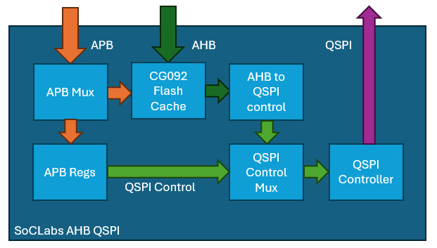
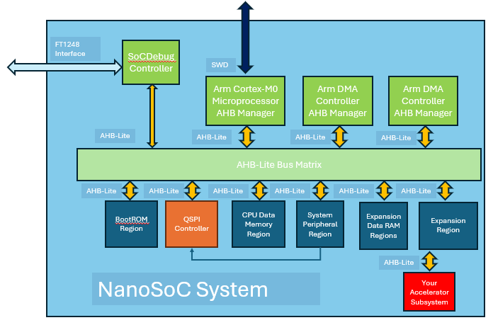
The fundamental design for the architecture is as below:
CG092 Flash Cache
The CG092 flash cache is a cache provided by Arm. It is instantiated between the bus interconnect and the flash controller to support caching. It has been optimised for fetching and caching instructions for M-class processors (particularly M3 and M4). The cache controller has a 32-bit AHB-lite subordinate that connects to the SoC bus, and a 128-bit AHB-lite manager that is connected to the "AHB to QSPI control block". The CG092 also requires an APB port for configuration of the cache controller
APB Mux
A simple APB mux from the Corstone 101. This is used to combine the CG092 apb interface and the internal APB register interface for the QSPI controller
APB Regs
This is used to configure the QSPI controller, and also to send configuration over the QSPI interface to the flash. This block is responsible for setting the clock frequency of the QSPI interface, the mode (SPI or QSPI), enable XiP mode, and to set some parameters of the AHB to QSPI control block. This is also the only interface that can write through to the flash over QSPI (as writing is more complex than reading)
AHB to QSPI control
This takes as input an AHB transaction, and converts to the QSPI control signals used to control the QSPI controller. This block can only read from the QSPI flash and will respond with a bus error if the SoC tries to write over this interface. It will also respond with an error if this interface is used to read over the QSPI, whilst the XiP mode is inactive.
QSPI Control Mux
Passes the QSPI control signals either from the APB controller or AHB controller. This is decided by the XiP mode, if XiP mode is active then the AHB interface is selected, otherwise it is the APB interface.
QSPI Controller
Main body of the AHB QSPI IP. This takes the QSPI control instructions and converts them to QSPI instructions. This is implemented with a state machine with the states: IDLE, NO_FETCH, OP, ADDR, MODE, DUMMY, DATA_O, DATA_I.
The QSPI controller has it's own line buffer. This is because the AHB interface can only send smaller than 128 bit transaction requests. This seems wasteful to fetch over QSPI. So QSPI will always fetch 128 bits when in XiP mode, and if the internal line buffer address matches the 128bit address (i.e. masking the least significant 4 bits) then it will not issue a QSPI transaction (i.e. NO_FETCH).
Verification
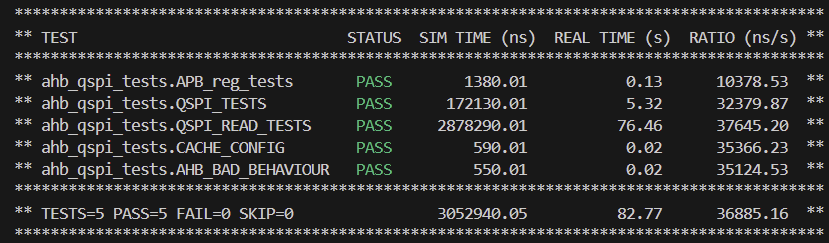
Initial verification of the subsystem. The simulation environment was setup using cocotb, using the AHB extensions to drive the AHB and APB ports of this design. The initial results for the coverage of the tests developed are shown below
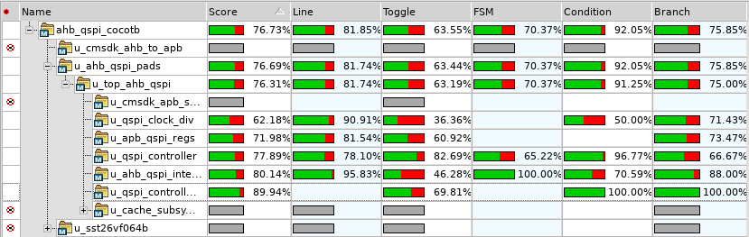
The average coverage from this is 76.73% (ignoring the arm IP coverage and sst26vf064b flash model). After examining the coverage report, some extra tests were added to the cocotb verification. These extra tests covered:
- FSM transitions in u_qspi_controller
- Toggle of bits like address, registers
- Tests to read uncovered branches
These additional tests were executed on a revised version of the sub-system with some tidying up of the implementation, particularly for registers that were too large (such as the clock divider register that was 8 bits, reduced to 5)
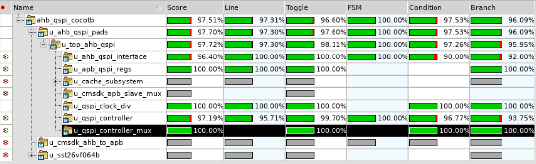
Coverage has so far been improved to 97.51%, with 100% coverage of the FSM in u_qspi_controller. Functionally, the tests are still passing, with assertions to ensure that it is functionally correct.
FPGA Implementation
For the FPGA implementation, a Pynq Z2 board was used with a PMOD SF3. This allowed for simple connection to the QSPI flash. In this case a micron MT25QL256ABA part was used so care had to be taken in order to ensure that the correct commands were sent.
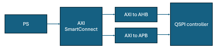
Additional wrappers were added as the PS of the Zynq board is native AXI, so a bridge from AXI to APB and AHB was required as shown below
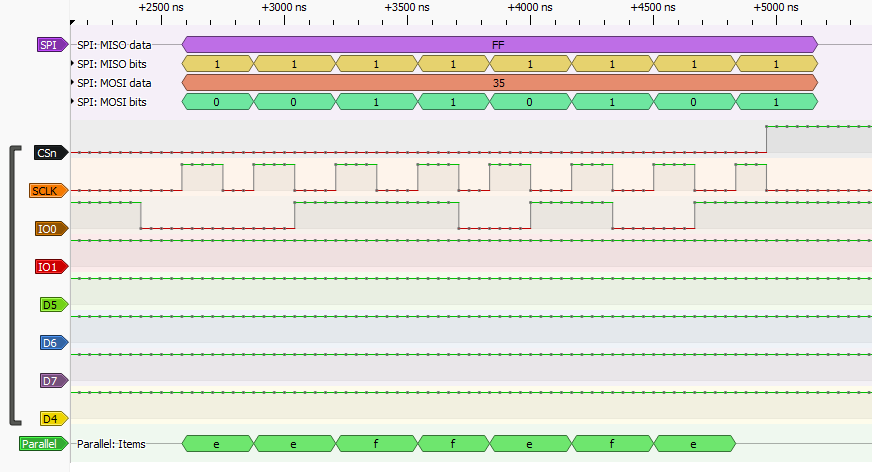
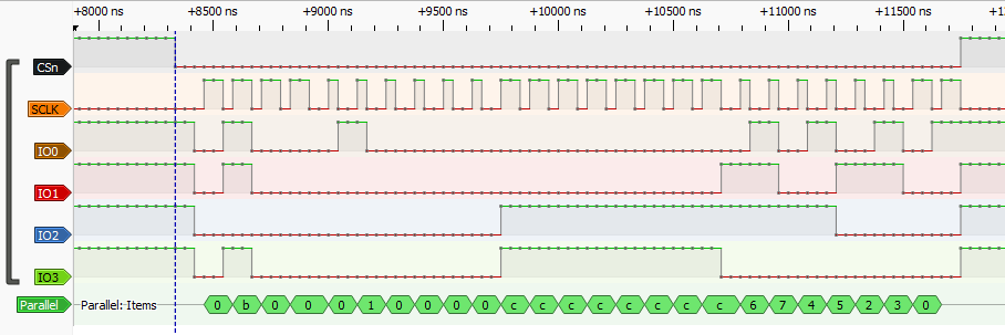
To ensure there was no effect on the timing of the FPGA, an external logic analyzer was used. Some of the verified behaviour is shown below from the logic analyzer. Firstly, a simple opcode transaction (0x35) which sets the QSPI flash in Quad I/O mode.
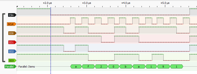
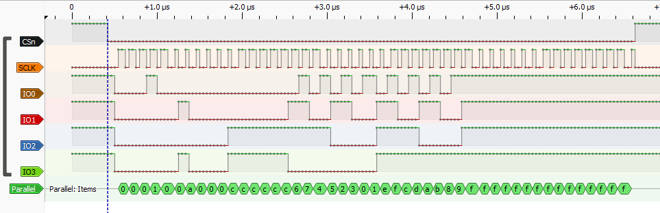
Then a QSPI read ID register transaction (0xAF). This shows that both the OP state and DATA in state are correctly working
Then a fast read command (0x0B). This was after writing to the flash so here is a test of the OP, ADDR, MODE, DUMMY, DATA I and DATA O states of the qspi controller
And lastly an XiP read over the AHB interface shows that the AHB controller working as expected
SoC Integration
Another verification test was to establish if a SoC design could boot from the QSPI flash. For simplicity, nanosoc is used here. In order to integrate into nanosoc, first the SRAM instruction memory had to be removed and replaced with an instance of the QPSI controller. Secondly the APB subsystem had to be edited to allow for control of the QPSI controller. And lastly top level pads/pins for the QSPI flash were added to the nanoSoC pad ring.
In behavioural verification the code is preloaded on the QSPI, and this works as expected. For the FPGA verification, the code has to be first written to the flash before it can boot.
The first method for programming the flash over FPGA is by using the ADP controller. This is similar to how the existing nanoSoC device is programmed, which is to write directly to the SRAM. However with the QSPI flash, writing has to be enabled, then data written from the controller buffer to the flash (currently only 16 bytes), wait until the flash has finished the write, polling the status register. Using the pynq environment of the Pynq Z2 board, this looks likes below:
file_stats = os.stat('hello.hex')
file_len_in_bytes = round(file_stats.st_size/3)
print(f'file size in bytes is {file_len_in_bytes}')
base_addr=0x0000
addr = base_addr
count = round(file_len_in_bytes/16)

start = time()
with open('hello.hex', mode='r') as file:
    for i in range(count):
        data = []
        for j in range(4):
            a=str.strip(file.readline())
            b=str.strip(file.readline())
            c=str.strip(file.readline())
            d=str.strip(file.readline())
            tmp = d+c+b+a
            data.append((int(tmp,16)))
        addr = base_addr + i*16
        print(data[0])
        QPI_WRITE_ENABLE(adp)
        QPI_PAGE_PROGRAM_128(adp, addr, data)
        while(QPI_READ_STAT_REG(adp)):
            pass

end = time()
length = end - start
print("Programming took " + str(length), "seconds")
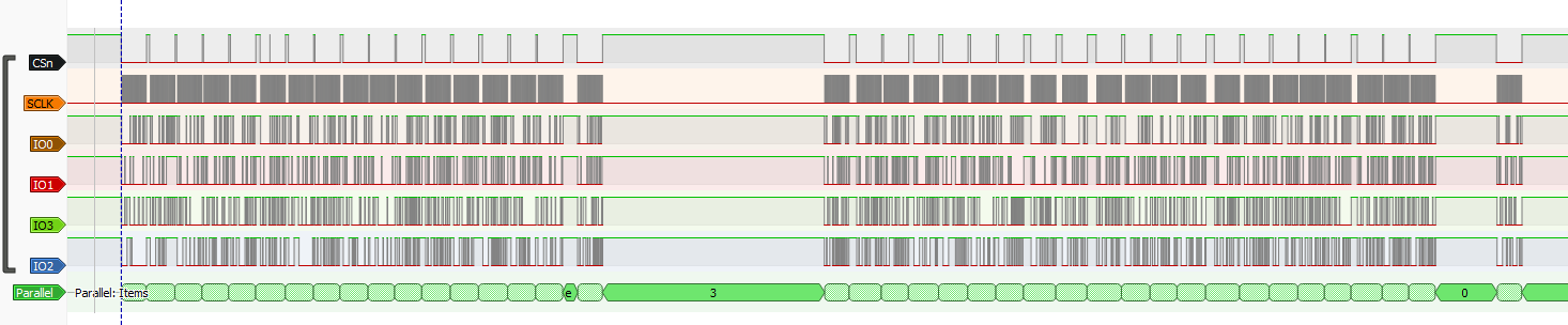
It has been verified that the test code runs as expected and the "Hello World" and "Test Passed" messages generated as expected. Below is the QSPI trace for running the hello world program
Physical Design
The plan is to tape out this IP as part of a nanoSoC miniASIC shuttle on TSMC 65nm. Before integrating this into the full nanoSoC design, some constraints for the IP are needed, and some idea on floorplanning.
This design has 3 clocks
- PCLK
- HCLK
- QSPI_SCLK
The QSPI SCLK is generated from the HCLK through a divider. But this is used as the clock internally in the QSPI controller. We must also ensure that the delays of the pins (both inputs and outputs) are clocked to same clock as seen on the output pin of the device.
For TSMC 65nm the constraints can be found here
Floorplanning
As this design uses some memory macros, supplying some recommendations around floorplanning is useful to the implementation engineers. Our initial floorplanning is shown as below
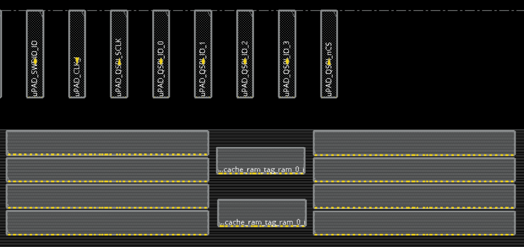
This places the SRAMs for the caches close to the pins (SCLK, IO[3:0] nCS). The 2 smaller SRAMs in the middle are the TAG rams for the caches.
From RTL to Silicon: What Physical Design Actually Means
By the time the AHB QSPI IP had been verified in simulation and tested on FPGA, the design existed only as synthesisable SystemVerilog — a text description of what the hardware should do, with no information about where transistors sit on silicon or how they are wired together. Physical design is the process of turning that description into a manufacturable layout: it decides which standard cells from the foundry's library implement each logic function, where every cell is placed on the die, how every wire is routed between them, and whether the result satisfies the foundry's manufacturing rules (design-rule checking, or DRC).
For this project, physical design targets TSMC 65nm LP (Low Power) using the 9-track tcbn65lp standard-cell library and is executed inside Synopsys Fusion Compiler 2022.12. Fusion Compiler is a unified RTL-to-GDS tool: it runs logic synthesis, placement, clock-tree synthesis (CTS), routing, and signoff checking in one environment, handing off a routed partition — a hardened block ready for chip-top integration — rather than requiring separate tools for synthesis and layout.
The hardened partition is named top_ahb_qspi. Its outputs (LEF, DEF, GDS, gate netlist, SDF, SPEF, SDC, UPF) are the deliverables that the chip-top integrator at IMEC plugs into the full nanoSoC die.
The Flow Architecture: Makefiles, Sentinels, and Stage Scripts
A real ASIC backend flow is not a single script that run once. It is a pipeline of stages where each stage can take minutes to tens of minutes and where a failure in one stage should not require rerunning everything from scratch. The top_ahb_qspi flow encodes this as a Makefile + sentinel-file pattern:
syn/asic/fusion-compiler/
├── Makefile ← orchestrates the whole chain
├── scripts/
│ ├── 1_init_design.tcl ← load RTL, libs, build floorplan, place macros
│ ├── 2_synthesis.tcl ← logic synthesis and initial placement
│ ├── 3_clock.tcl ← clock-tree synthesis (CTS)
│ ├── 4_route.tcl ← global + detail routing
│ ├── 5_signoff.tcl ← timing/design signoff checks
│ ├── pg_mesh.tcl ← M5/M6 power strap mesh definition
│ ├── pg_prestitch.tcl ← macro power ring pre-stitch (pre-route)
│ ├── pg_rails.tcl ← std-cell VDD/VSS rail compile (post-route)
│ ├── 6_partition_export.tcl← hand-off package: LEF/DEF/GDS/SDF/SPEF/UPF
│ └── 7_drc.tcl ← signoff checks and bounded waivers
└── syn/asic/
├── common.mk ← shared PDK paths (the file that bit us — see below)
└── pdk_paths.tcl ← Liberty .db, TLU+, LEF paths
Each stage, when it completes successfully, touches a sentinel file (.init.done, .synth.done, …). The Makefile uses these as dependency targets, so the dependency chain is:
.init.done → .synth.done → .cts.done → .route.done → .pg.done → .signoff.done → .drc.done → .abstract.done → .lec.done
Stage1 - Init Design
This is the setup stage. Before synthesis or placement can begin, Fusion Compiler needs to know the physical and electrical properties of every building block it will use. This script:
- Loads the Liberty
.dbtiming libraries for the TSMCtcbn65lpcells — one for each operating corner (slow/fast, different voltages and temperatures). These files encode propagation delays, setup/hold times, and power for every cell in the library. - Loads TLU+ parasitic models, which capture the resistance and capacitance of metal interconnect at this process node. Without these, timing and power estimates during PnR would be inaccurate.
- Reads the LEF abstracts for the two precompiled memory macros —
flash_cache_dataandflash_cache_tag— that implement the Arm CG092 Flash Cache. LEF abstracts describe a macro's physical footprint and pin locations without revealing its internal layout. - Elaborates the RTL (
top_ahb_qspi.svand its hierarchy), links the design to the loaded library, and sets up MCMM scenarios (Multi-Corner Multi-Mode): one scenario for slow-corner setup timing analysis, one for fast-corner hold timing analysis. Both scenarios are active throughout the flow, so timing is always checked against both extremes simultaneously. - Initialises the floorplan: die size 980 × 240 µm, core offset 10 µm, and places the two SRAM macros into their pre-determined locations (described below in the Floorplan Details section).
- Constructs the power grid — horizontal and vertical mesh straps on M5 and M6 that will carry VDD and VSS from the partition boundary down to every cell.
A good rule of thumb: if Init fails, the problem is almost always a missing library file, a wrong PDK path, or a macro the tool cannot find. Everything else — timing, DRC — is downstream of getting this stage right.
Stage2 - Synthesis and Placement: Gates from RTL
This the stage where RTL description becomes a gate-level netlist. Fusion Compiler's compile_fusion command runs in three sub-phases:
logic_opto— purely logical: the tool maps the RTL operators and registers to cells from thetcbn65lplibrary, optimising for timing and area without yet worrying about physical location. After this phase you have a flat, unplaced netlist.initial_place+initial_opto— the tool places cells onto the floorplan grid and re-optimises timing with placement information in hand. Wire length now affects delay estimates, so cells that need to talk to each other get pulled closer together. The clock is treated as ideal at this stage (the real clock tree is built in Stage 3).final_place— a final placement legalisation pass, after which the tool reports route congestion. High congestion here is a warning: it means the placer had to pack cells too densely in some region, which the router will struggle to escape. Fortop_ahb_qspi, the macros dominate most of the die area, so standard-cell congestion is concentrated in the central channel between them — a channel that later caused a DRC issue (described below).
An important choice made in this stage is the dont_use constraint on scan-capable flop variants (SDF*, SEDF*, GSDF*). By default, Fusion Compiler is free to map registers to scan flops because they are present in the library. This partition does not build scan chains, so scan flops would have their SI/SE pins tied to constants — and those constant-distribution nets created persistent routing shorts. Setting dont_use on scan cells in scripts/setup_design_options.tcl prevents this. A future DFT flow can re-enable them with FC_ENABLE_SCAN_CELLS=1.
Stage3 - Clock Tree Synthesis
Until now, the clock has been treated as a single, zero-skew ideal wire reaching every flip-flop simultaneously. In reality, a clock signal must be physically distributed across the die through a tree of buffers and inverters, and each branch of that tree has real propagation delay. Clock-tree synthesis (CTS) builds this physical distribution network. This stage is executed in three sub-phases:
clock_design— the tool drafts the initial clock tree topology, inserting buffer/inverter cells to drive the fanout from the clock source to every register's clock pin.final_opto— timing optimisation with real (non-ideal) clock delays now in the timing graph. Setup slack is re-checked with the actual clock arrival time at each endpoint.route_clock— the clock distribution wires are routed on preferred upper metal layers (lower resistance = less clock uncertainty).
Hold violations are a phenomenon that is only physically meaningful after CTS. Before CTS, every flip-flop sees the clock at time zero, so hold is trivially satisfied everywhere. After CTS, some flops see the clock slightly earlier than others due to tree imbalance — and a flop that clocks earlier on the capture side than on the launch side can capture stale data (a hold violation). Fixing hold means inserting delay — small buffers — on the paths that arrive too fast.
This design has three clock domains: PCLK (APB), HCLK (AHB), and QSPI_SCLK (generated from HCLK through a divider inside the RTL). The SDC constraints declare the QSPI_SCLK crossing as asynchronous, so the tool knows not to apply inter-domain timing constraints across it.
Stage4 - Routing
This stage is also executed in three phases,
route_auto— global routing followed by detail routing. Global routing assigns each net to a sequence of routing tiles; detail routing assigns actual track coordinates and inserts vias. The router uses the metal stack defined by the TSMC 65nm technology file (M1 through M9 for signal, M5/M6 for the PG mesh).route_opt— post-route timing optimisation: small buffer insertions and gate resizing to fix timing violations that appeared after routing added real wire resistance to delay calculations.
Hold fix scoped to the fast corner — hold violations are fixed at this stage, explicitly targeting the fast-corner scenario only. Fast-corner analysis uses low-resistance metal and fast transistors, which is exactly the condition where launch paths can race ahead of capture paths.
Iterative DRC cleanup — if route_auto leaves any DRC violations (shorts, spacing, minimum area), the script runs route_detail -incremental true in a loop, giving the router additional attempts to resolve local conflicts. In a macro-dense layout like this one, the router sometimes needs ECO placement relief (slightly moving standard cells) to escape a congested corner. If the loop reaches the iteration limit with remaining violations, the flow proceeds and the residual count is caught at Stage 7 DRC.
Stage5 - Power/Ground Rail Compile
After routing, the power grid straps and the standard-cell VDD/VSS rails are rebounded together through a compile_pg step. This is not a single numbered stage script but a dedicated make target (make fc_pg) backed by a set of helper scripts: pg_mesh.tcl defines the M5/M6 strap mesh, pg_prestitch.tcl pre-stitches macro power rings before routing, and pg_rails.tcl compiles the final std-cell VDD/VSS rail connections after routing completes. Together they ensure that every cell's power pins are physically connected to the nearest strap, and that any PG geometry that shifted during routing ECO is still correctly connected.
The macro PG straps — the horizontal M5 connections that bring power into the SRAM macro power rings — are stitched here with a pitch of 4.5 µm. This specific pitch was arrived at through debugging (described in the next section); looser pitches left EOL DRC violations, tighter pitches caused other geometry conflicts.
Stage6 - Partition Export
This stage assembles everything the chip-top integrator needs.
| File | What it is |
|---|---|
top_ahb_qspi.lef | Physical abstract: footprint and pin shapes for chip-top P&R |
top_ahb_qspi.def | Full routed layout database |
top_ahb_qspi.gds.gz | GDS stream (partition geometry — see caveat below) |
top_ahb_qspi.v | Gate-level logic netlist |
top_ahb_qspi.pg.v | Gate-level netlist with PG pins for LVS |
top_ahb_qspi.sdc | Timing constraints re-exported for chip-top STA |
top_ahb_qspi.upf | Power intent for chip-top multi-voltage flows |
top_ahb_qspi.scen_slow.sdf | Slow-corner back-annotated delays |
top_ahb_qspi.scen_fast.sdf | Fast-corner back-annotated delays |
top_ahb_qspi.scen_*.spef* | Extracted parasitic data per corner |
A note on the GDS — what it contains and what it doesn't
top_ahb_qspi.gds.gz is not a fully merged tapeout GDS. This is a normal and expected boundary in partitioned flows, worth understanding clearly.
The TSMC tcbn65lp standard-cell back-end GDS stream — the file containing the actual polygon-level layout of every gate in the library — is licensed IP that is not available on every build host. Fusion Compiler produces a correct routed GDS for all geometry it does have: the partition's metal layers, vias, and the two precompiled SRAM macro layouts (flash_cache_data and flash_cache_tag), which are included. For the standard cells, it skips the merge and logs a clear warning rather than silently omitting them.
The missing standard-cell GDS layer must be merged at the final integration step where the correct PDK licence is available. IMEC will merge it during chip-level GDS assembly, LVS, and signoff DRC. This is the intended hand-off boundary — not a flaw in the partition closure.
Satge7 - DRC Summary
In this stage a structured set of checks are performed and makes a pass/fail decision before any subsequent stage can run. The checks, and the final results,
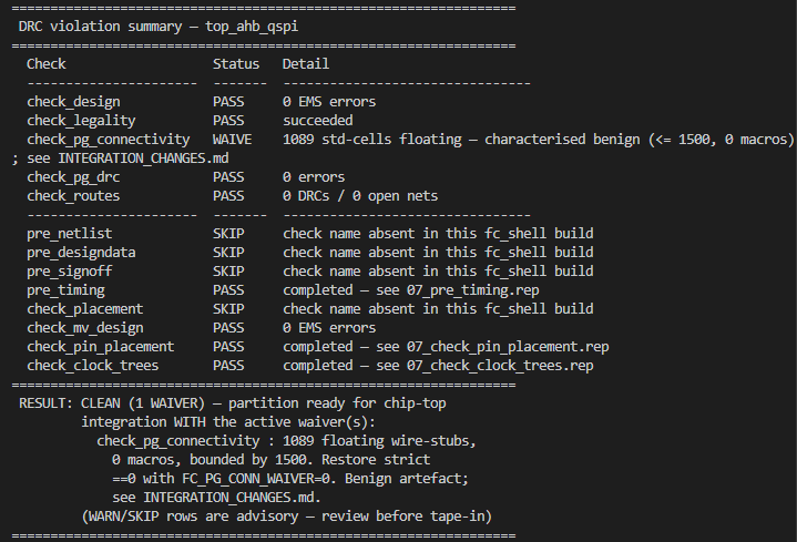
The one waiver — check_pg_connectivity — needs explanation, because it looks alarming until you understand what it is and is not saying. The check reports 1,089 floating standard-cell PG wire-stub objects. These are short PG wire fragments at the partition boundary that the tool flags as potentially disconnected. Crucially, floating hard macros = 0: both SRAM macros have fully verified power connections. The floating count was reproduced identically by re-running the post-route PG compile in isolation (make fc_pg_probe), which confirms it is a reporting artefact of the partition-level mesh boundary rather than a real disconnect inside the partition. It is waived here and will be resolved when the partition is wired to the chip-top global VDD/VSS rails during integration.
Formality LEC: Proving the Netlist matches the RTL
Logic equivalence checking (LEC) is the formal proof that the gate-level netlist Fusion Compiler produced is functionally identical to the original RTL — that synthesis did not accidentally drop a logic cone, invert a condition, or introduce a latch where there should be a register. Synopsys Formality runs the proof automatically as the final step of fc_all.
1,805 compare points is the count of individually verified output/register boundaries. Zero failures means the synthesis result is formally equivalent to what was simulated and verified.
Two DRC bugs:
Issue 1: Scan Flops Without a Scan-Chain Flow
Fusion Compiler's library contains scan-capable flip-flop variants (SDF*, SEDF*, GSDF*) — flops with extra SI (scan-in) and SE (scan-enable) pins used in Design-for-Test flows to chain all registers into a scan path for manufacturing test. The tool is allowed to use them by default because they sometimes offer marginal timing advantages over their non-scan counterparts.
This partition does not implement a scan chain. So when Fusion Compiler selected scan flops, it tied the unused SI/SE pins to constants through new tie-cell networks. Those networks added short, dense distribution wires in areas already being used by signal routing — and caused persistent local routing shorts that could not be resolved by the router's DRC cleanup loop.
The fix: add dont_use attributes to all scan-cell variants at the start of synthesis (scripts/setup_design_options.tcl). This takes one Tcl command and prevents the problem entirely. A future DFT flow that genuinely builds scan chains can re-enable them with FC_ENABLE_SCAN_CELLS=1 — at which point the ScanDEF and scan-stitching infrastructure also needs to be present.
The lesson here is general: if you are not running a specific EDA sub-flow (DFT, power gating, retention registers), explicitly exclude the cells that only make sense in that sub-flow. The library is comprehensive; the tool does not know which parts of it your flow intends to use.
Issue 2: M5 End-of-Line Keepout Violations from Macro Geometry
Once the scan-flop issue was resolved, signal routing closed cleanly — but check_pg_drc still reported M5 end-of-line (EOL) keepout violations. The log messages included lines like Layer M1 pitch 0.200 may be too small: wire/via-up 0.225. (ZRT-026)
The instinct when you see a message like that is to suspect the technology file is misconfigured. It was not. Fusion Compiler was correctly enforcing real TSMC 65nm design rules; the geometry violating them was in the floorplan, not the rule deck.
The physical cause: the two side SRAM macros (flash_cache_data) sat close to the die edge, with horizontal M5 power straps running over vertical M4 macro pins in a narrow strip. Because the die edge was close, these M5 straps were forced into short fragments near the edge — fragments short enough to trip the M5 EOL keepout rule.
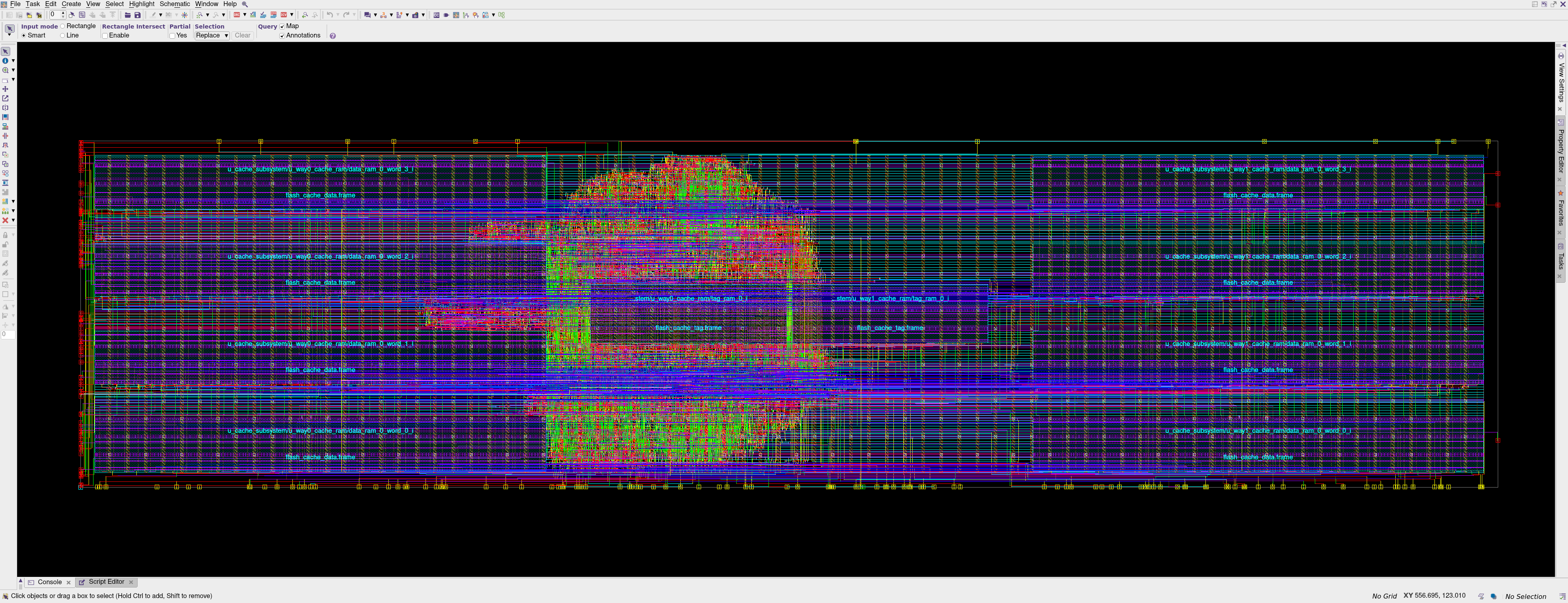
The investigation followed a clear pattern: changing macro placement changed the DRC count; changing M5 mesh offset changed the DRC count; restoring the central routing channel while widening the die fixed both. That behaviour points to floorplan topology, not a bad technology file.
| Parameter | Final value | Why |
|---|---|---|
| Die width | 980 µm | Wider than the previous 970 µm to compensate for moving macros |
| Die height | 240 µm | Unchanged |
| Core offset | 10 µm | Standard boundary |
| Side macro margin | 0.0 µm | Macros placed directly on the core boundary to eliminate the edge strip |
| Vertical macro channel | 20 µm | 100 M1 tracks — enough via-up headroom for the 86-bit cache bus |
| M5 mesh offset | 12.5 µm | Aligns strap starts away from macro pin columns |
| M6 mesh offset | 10.0 µm | Complementary alignment on the orthogonal layer |
| Macro PG strap pitch | 4.5 µm | Dense enough for connectivity, sparse enough to avoid EOL fragments |
Conclusion:
The top_ahb_qspi partition is one IP block among several in the nanoSoC miniASIC shuttle, targeted for tape-out on TSMC 65nm in July 2026. The chip-top integrator at IMEC assembles all partitions into the full die, applies the chip-level power grid, runs full-chip DRC/LVS, and submits to the foundry.
By hardening top_ahb_qspi as a partition first, the flow gives the chip-top a pre-characterised block: its timing is known (via SDF/SPEF), its power intent is declared (UPF), and its physical boundary is fixed (LEF/DEF). The chip-top STA can treat it as a black box or use the NDM block directly for hierarchical timing analysis. That separation of concerns — timing-close each IP independently before integration — is how large SoC projects remain manageable.
The items that remain open for IMEC integration are:
- Merge the missing
tcbn65lpstandard-cell GDS stream into the full-chip GDS - Run chip-level Calibre DRC/LVS/antenna with the correct foundry runsets
- Wire partition VDD/VSS to chip-top global rails (resolving the PG waiver)
- Run IR-drop and electromigration analysis on the chip-top PG mesh
- Validate the ETM extracted timing model against silicon, or use the
.dlibNDM block for hierarchical STA
Each of these is a normal deliverable at the partition-to-chip-top boundary — not an indication that the partition is incomplete. The partition itself is clean: 0 route DRCs, 0 open nets, 0 PG DRCs, Formality LEC passed.
Project Milestones
Do you want to view information on how to complete the work stage ""
or update the work stage for this project?
-
Architectural Design
Design FlowTarget DateCompleted DateHigh level architecture of the AHB QSPI
Result of WorkDone, image for the architecture added to page above
-
Getting Started
Design FlowTarget DateCompleted DateSetup environment for the AHB QSPI IP
Result of WorkEnvironment setup with the Arm IP, simulation environment using the SoCtools git
-
IP Selection
Design FlowTarget DateCompleted DateResult of WorkArm IP used is the CG092 and some of the corstone 101 for the bus infrastructure
-
Behavioural Design
Design FlowTarget DateCompleted DateTake the architectural model and develop the behavioural model
Result of WorkHDL created for the IP
-
Simulation
Design FlowTarget DateCompleted DateSetup the simulation environment and run the initial verification
Result of WorkCompleted simulation with no bugs. Initial verification coverage averages 76.73%
-
Logical verification
Design FlowTarget DateCompleted DateVerify the design, functionally and with coverage
Result of WorkDesign has been verified with coverage of 97.5%
-
RTL Verification
Design FlowTarget DateCompleted DateResult of WorkTested on FPGA with integration in nanoSoC, SoC boots code over the QSPI Flash interface
-
Tape Out
Design FlowTarget DateCompleted DateTarget to tape this out on a TSMC 65nm miniASIC shuttle as part of the nanoSoC chiplet tapeout
Result of WorkSent off for tapeout Sept 2026. Waiting on silicon back now.
This was as part of the nanoSoC ethernet chiplet, there will be another tapeout of the IP inside the nanoSoC compute chiplet, expected to tapeout Nov 2026 -
Verification Methodology
Design FlowTarget DateCompleted DateVerification uses multiple QSPI models as the VIP (micron model and microchip model)
Further verification could be enhanced with protocol checkers using Synopsys VIP -
Physical Verification
Design FlowTarget DateCompleted DateDRC, LVS, ERC checking
Result of WorkAs part of the nanoSoC Ethernet chiplet tapeout this has all be verified and complete
-
Timing closure
Design FlowCompleted DateResult of WorkAs part of the nanosoc ethernet chiplet tapeout. Timing has closed at 100 MHz on TSMC 65nm.
-
Routing
Design FlowCompleted DateResult of WorkComplete as part of the nanosoc ethernet chiplet tapeout. No specific issues found for this step
-
Clock Tree Synthesis
Design FlowCompleted DateResult of WorkComplete as part of the nanosoc ethernet chiplet tapeout. No specific issues found for this step. Constraints for this have already been verified in synthesis and FPGA. The only slight complication is the generated clock from the clock divider, although in the taped out design we don't expect to use the clock divider as the system frequency is less than 100 MHz (same as the max frequency for the flash chips we are targeting)
-
Floor Planning
Design FlowCompleted DateResult of WorkFloorplanning on TSMC 65nm complete. Macro placement and power routing are the main issues although fairly straightforward. Automatic floorplanning was used for the tapeout of nanosoc ethernet chiplet, to try and provide best timing over a more area constrained chip
-
Synthesis
Design FlowCompleted DateResult of Workdetails added on synthesis complete. The main constraint here was making sure scan-capable flops aren't introduced in case we do want to use scan chains in the future
-
Technology Selection
Design FlowCompleted DateResult of WorkInitial flow and tapeout for this done on TSMC 65nm. Although support for other nodes is feasible as the only macros at the moment are SRAMs

Team

 Project Creator
 Daniel Newbrook
Digital Design Engineer
at University of Southampton
Research area: IoT Devices
ORCID Profile
 Corstone 101 for m0/m3
 SPI/QSPI
 Hardware design
Submitted on
Comments
Tape Out plan
Hi,
Is there a target tape out for this IP?
John.
Tape Out Plan
Hi John
Yes we do have a tape out targeted for this IP. I'm going to add some more detail to the project soon on this subject.
The plan is to tape out nanoSoC with this IP integrated in July 2026 on a miniASIC shuttle. We have already tested and verified the integration of the IP in nanoSoC and shown it to be working on FPGA. I will add some more detail about the backend floorplanning and constraints for this IP to this project
Daniel
New date
Hi,
I see we missed the expected date for this milestone. Perhaps we can put in a new one.
John.
Comparison of Non-Volatile memory
If anyone is interested in the relative merits of the different types of NVM then this article by Tim Daulby might be helpful.
Add new comment
To post a comment on this article, please log in to your account. New users can create an account.