nanoSoC 2023/4
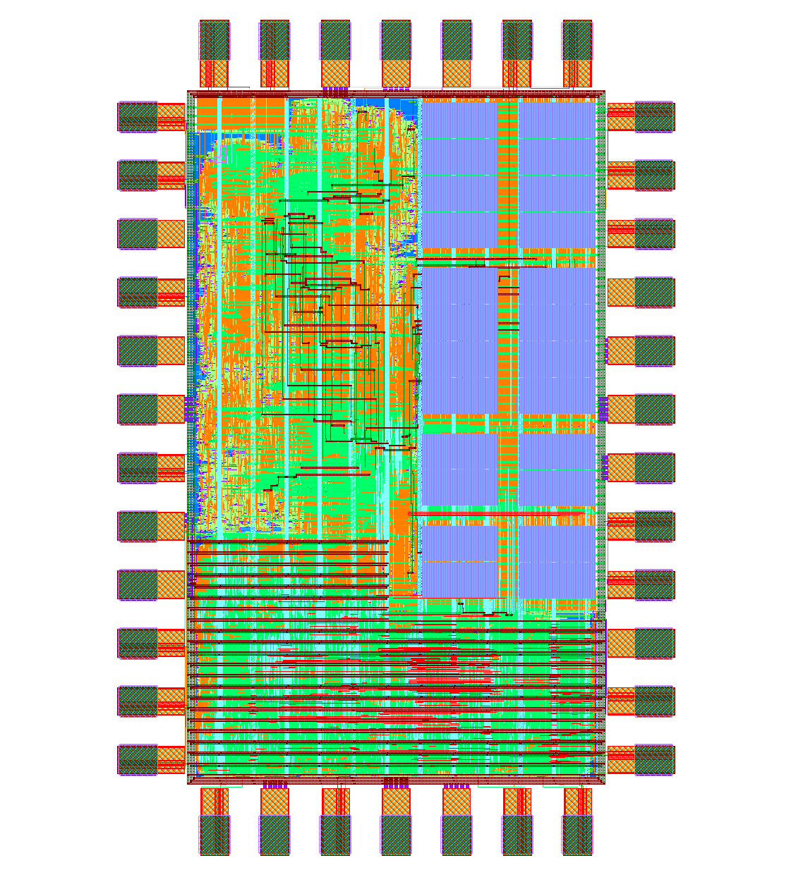
The first tape out of the nanoSoC Cortex M0 based SoC Reference Design. This reference design provides a simple microcontroller system appropriate to host and support the development and evaluation of research IP blocks or subsystems. It supports seamless transition from FPGA to physical silicon implementation utilising a memory-mapped experimental hardware subsystem.
The SoC is configuratble and includes a Cortex-M0, boot monitor, Instruction and Data SRAMs, system peripherals (UART, GPIO, system counter timers and clocks), memory mapped expansion space (for experimental IP), 2-banks of SRAM expansion region, a DMA (either PL230 or DMA350 supported) and an ASCII debug protocol agent (or ADP).
The 2023/24 version of the reference design has been used to tape the following projects to date:
- Fast-kNN: A hardware implementation of a k-Nearest-Neighbours classifier for accelerated inference by Epifanios Baikas
- Hell Fire SoC by Srimanth Tenneti


 Cortex-M0
 CoreLink DMA-230
Comments
nanoSoC test board
Both of the projects used the same package and can be tested using the same reference test design board, see here.
Add new comment
To post a comment on this article, please log in to your account. New users can create an account.