ARM Cortex M0 Based SoC for Biomedical Applications
Conventional healthcare is expensive and reliant on the physical presence of the patients. Continuous health monitoring tracks vital health parameters like heart rate, blood pressure, etc. While these work well in measuring the parameters, modern-day devices rely on the cloud to compute and interpret data. This results in an increase in data transfer between the device and the cloud, and if this connection breaks, there can be no interpretation of data. Hence, there is a need to shift the computation to the hardware, referred to as "Edge Computing".
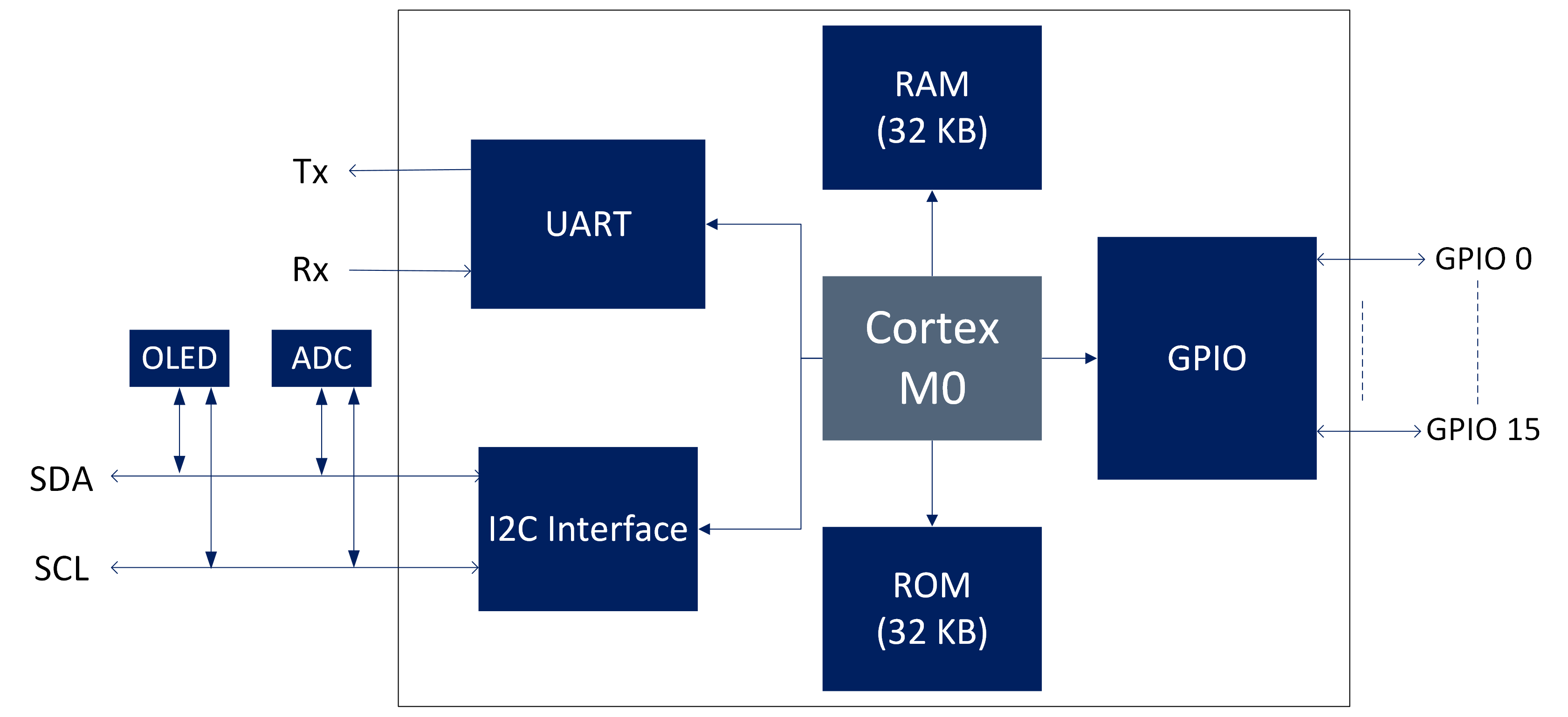
In this project, we implement a Cortex M0-based SoC that is used to monitor the heart rate continuously. The SoC takes the data from the photoplethysmograph (PPG) sensor and displays the heart rate on the OLED display after processing.
Project Milestones
Do you want to view information on how to complete the work stage ""
or update the work stage for this project?
-
Architectural Design
Design FlowTarget DateCompleted DateIn this milestone, we aim to define the hardware used in the SoC. Behavioural level code has been written in Verilog to allow protocol conversion between AHB Lite protocol used in ARM Cortex M0 and UART/I2C peripheral.
-
Architectural Design
Design FlowTarget DateCompleted DateAfter defining the customized hardware for the UART and I2C interfaces, we develop customized software. This will help the user and programmers to work with the SoC without worrying about the underlying hardware.
-
FPGA Prototyping
Target DateCompleted Date- In this milestone, we aim to test Xilinx's proposed hardware and software on Basys 3 FPGA.
- PMOD ports on Basys 3 were used for the I2C interface.
- To the PMOD port, we connect two wires for I2C connections: one for SDA and one for SCL I2C port.
- Both the ports were connected to the breadboard and to the PPG and I2C interface.
-
Synthesis
Design FlowTarget DateIn this milestone, we will use Cadence Genus to compile our design using 90 nm libraries.
Team
PhD Scholar
at Indraprastha Institute of Information Technology
Research area: Multicore Architecture
 Cortex-M0
![]() Hardware design
Hardware design
Submitted on
Comments
Updates on Milestones
Hi,
As we are now into the start of October it would be good to get an update on your milestones at the end of September.
We need to understand if it is likely you will be making progress so we can progress a tape out.
If you need any help or support for the project please let us know.
We look forward to hearing from you.
90nm tape out
Thanks for adding the latest milestone on the synthesis using 90nm libraries. Have you obtained foundry specific libraries?
Tape out on mini ASIC
Just to add to this, Europractice don't support a 90nm mini ASIC tapeout.
As reference we have recently taped out some dies with nanoSoC using TSMC's 65nm mini ASIC shuttles with a 1 x 1.5 mm size so this may be a better technology node to target, but happy to discuss this with you further
Updates to milestones (end of May 2024)
Hi,
It would be good to get an update on your milestones at the end of the month.
John.
Updates to milestones (end of June 2024)
Hi,
As we are now into the start of July it would be good to get an update on your milestones at the end of June. If you need any help or support for the project please let us know. We look forward to hearing from you.
John.
Thank you for the updated milestones
Hi,
Thanks for the updated milestones. If you need any help with the Synthesis then please let us know.
John.
Analog or digital sensors
Can you help define what type of photoplethysmograph (PPG) sensor you intend to attach to the SoC.
Daniel has now published a mixed signal subsystem reference design project to extend the nanosoc reference design to add analog to digital conversion using the APB peripheral bus.
Hopefully this will help you with your Architectural design.
Analog or digital sensors
Daniel has now updated the mixed signal subsystem reference design project, you might want to follow that project as a way to help with your own Architectural Design?
Adding new milestones
It is very easy to add new milestones and you can come back as each milestone progresses and make updates.
IITH are a good example of milestones in their project https://soclabs.org/project/real-time-edge-ai-soc-high-speed-low-complexity-reconfigurable-scalable-architecture-deep
You can simply select milestones from the generic design flow stages or create any unique milestones. So taking the first steps in the design flow you type 'arch' and it autocompletes the design flow step needed.
Progress of SoC Hardware Design milestone
Thank you for your initial milestone of SoC Hardware Design. You had a target of the end of April How did that go?
I see this initial milestone to be much like the generic flow Architectural Design stage which currently has three sub-stages:
Specifying a SoC
So this is aligned to your 'aim to define the hardware used in the SoC'. I think will also help to think about the data rates and flows through the system.
IP Selection
Pick the IP parts from the Technology section. You have listed the main M0 processor IP. What IP will you adopt for other functions. I was interested to hear that you had 'written in Verilog to allow protocol conversion between AHB Lite protocol used in ARM Cortex M0 and UART/I2C peripheral' . Do you plan to use the PL011 UART IP block and adopt the APB bus? or are you taking a different design plan?
You might also want to think about your Project Structure and other high level Design Flow considerations.
Verification
You should start to think about how you will validate your SoC design. Creating verification and validation assets as you develop the design is a good working practice.
You should find some helpful examples from some of the other SoC Labs projects.
Happy to help and answer any questions.
Example of how to update a milestone
Here is a good example of update to a milestone to add a completion date and show progress. It comes from one of last years projects.
It shows both the Completed Date and key additional information such as the reported area with a clear statement of the inputs that this is not using a specific technology node standard cells.
Add new comment
To post a comment on this article, please log in to your account. New users can create an account.