
Floor Planning
Introduction
The floorplan of your System on Chip ("SoC") design lays out all of the parts of the system in a way that provides optimal flow of signals and power delivery, that makes best use of energy and chip area, while delivering the best performance. Industrial designs that are very cost sensitive may have many design iterations to get an optimal layout that will make significant cost benefit when fabricated millions of times. Academic tape outs are not likely to have such optimisation demands but can still benefit from careful floor planning.
Floor planning has until recently been a mainly manual design task but major tool providers are developing design assistance for this activity. It is an important step in the Physical Design process as it the chosen floorplan layout has effects on the rest of the steps in physical design including placement and routing. Like many engineering tasks it is making trade offs between various factors such as total area, wire lengths, aspect ratios of any fixed macro structures, timing, etc.
The floor plan needs to take into account any external constraints in terms of the expected packaging of the SoC design. The interface to the external environment in terms of both pin counts and pin placement can have a significant effect on the floor plan layout.
The floor planning design task optimises the placement of all the components, connection pads, macros, standard cells, power, ground, etc, taking account of physical constraints such as minimal area, separation, interconnect lengths, power as well as timing and other considerations.
Top level constraints
Die Area / Floorplan Aspect Ratio
Fabrication of devices differs by manufacturer and they can have specific constraints on the size and shape of the physical die as well as the external connection s via pads depending on the type of physical connections to be made. Some foundry partners have different rules for adjusting the x and y dimensions of final die and cost can also constrain the choices made for the technology selection and foundry.
External Pin Placement
Placing of the external connections can have constraints imposed by the external environment, the type of package, the choice of interconnect protocols in the SoC design and the physical interactions that may occur between signals as well as the internal physical design aspects of floor plan and routing decisions.
System Architectural considerations
The design decisions made at the Architectural Design stage will impact on the floor planning activity as will the choice of system IP components.
Memory Considerations
Memory tends to have rigid aspect ratio and size constraints. Memory can be a significant proportion of the die area and may also have important high speed interconnections to other parts of the system and the external environment that need special consideration.
Pad ring design
The pad ring is the circuitry that surrounds the die to enable off-chip connections. This is formed as a 'ring' or 'frame' due to the fact that internally each pad cell will have buses for power and ground that when they are all connected together, will form a ring around the die.
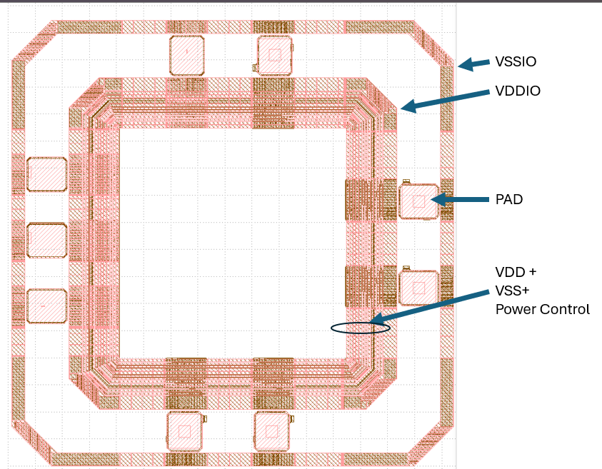
You can see in the above image a very simple pad-ring using the Skywater 130 PDK. In the ring there are routes for the IO power and ground, as well as core power and ground and some power control signals that are supplied to each pad.
Internally, each pad driver circuit can be composed of
- Digital buffers
- ESD protection
- Power control circuitry
- Drive strength circuitry
- Pull up/down control
These are composed of mostly the same transistors as in the core of the design, however typically some thick-dielectric transistors will be used for the IO voltage.
Building a Pad ring
The procedure for this is as follows:
- Specify the number of IO's and types you need for your design
- GPIO generally for digital, but the PDK may have many options in terms of drive strength, directionality, speed etc.
- Analog pins may have dedicated IO circuitry (generally just a wire with ESD protection)
- Calculate required power and ground
- If you just need a single IO power domain, this is fairly straighforward. For the IO supply you may typically need around 1 power+ground pair for every 4-6 pads that you have. Usually though the PDK/IO library will supply information to calculate this accurately
- Sometimes you need to cut the IO power domains up (or if you have seperate core domains supplies, maybe seperate the ring for this reason). There may be some "cut" cells available, alternatively for separate core domain supplies, there may be some power/ground pads that do not connect to the pad ring (usually refered to as macro supplies)
- Make a layout
- Spread power and ground supplies as evenly as possible
- Speed critical pads should probably be as close to the internal circuitry as possible.
- Clump together related pins (i.e. QSPI pins all together)
At this point you need to make sure the spacing between pads is sufficient for your bonding process (wire or flip chip). These details are available from your bonding house or europractice
Other Considerations
Power Distribution
It is important to ensure power delivery to the various parts of the system to minimise dynamic voltage drop in order for the design to operate at the required frequency. There is an important relationship between the supply voltage and propagation delay in logic circuits. If supply voltage is not maintained current flow through the transistors is affected and so the switching speed of the logic. Some parts of the system, such as the processor are known to have high switching activity. Simultaneously switching of logic in closely connected space can cause a sharp demand for current in that area. A hard macro in isolation might pass voltage drop margin requirements, but in close combination with other logic might not.
Like other design tasks, the design of the power network follows a hierarchical decomposition and also design iterations. Tool vendors have power analysis tools to assist.
Signal Integrity
Identifying the critical signal paths in a design can help floor planning decisions. Prioritising the placement of these signal paths can affect relative placement of component parts in the overall system. Allocate sufficient floor plan area for routing signals to avoid congestion and signal crosstalk can be important. Having a good layout for global routing layers can improve the results of later place and route activity.
Analog signals can be more susceptible to noise, decoupling signal tracks from those of neighboring signals can help maintain signal integrity.
- NanoSoC floor planning considerations
The nanoSoC reference design is a simple microcontroller based SoC design. With nanoSoC the more important considerations where to place the memory instances which were a significant portion of the area, the external connections, and the routing of power domains.
Die Area / Floorplan Aspect Ratio
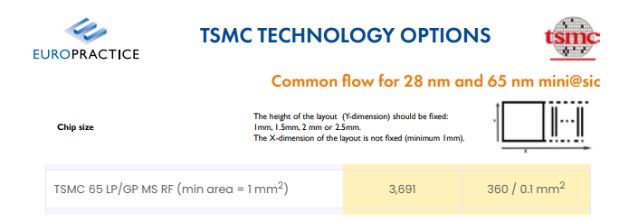
One of the target aims for nanoSoC was a low cost of fabrication of devices. Initial devices were fabricated using the Europractice which provides a range of fabrication paths. For the low cost miniASIC path additional area can be added in 0.1mm but while the x dimension is flexible, the y direction is in larger fixed increments.
External Pin Placement
One of the target aims for nanoSoC was to keep the external connections to a small number in order to keep packaging costs and the cost of the external test board to a low cost.
System Architectural considerations
The first nanoSoC tape outs were to support the addition of academic projects on custom accelerators. The M0 processor within the Arm Academic Access programme is a small gate count soft IP. In more complex SoC designs the processor subsystem might be a significant constraint to the floor planning.
Memory Considerations
Memory tends to be a significant factor in early nanoSoC designs that focused on the addition of custom accelerators for Artificial Intelligence / Machine Learning. It is important to keep signal paths for on-chip memory to the accelerators short. Instruction and data memory blocks as well as boot ROM is accessed by the M0 processor within the nanoSoC reference design.
The SoC Architecture, along with decisions on the use of separate power domains for the main processor part and separately the custom accelerator gave direction to placement of memory blocks, within the overall aim of trying to utilise the die area effectively.
- Cadence
This example flow uses Cadence for the SoC labs FT1248 to axi stream components based on the open source Global Foundries 180nm PDK..
Die Area / Floorplan Aspect Ratio
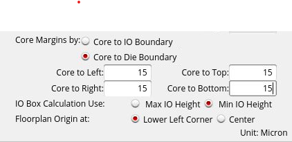
It may be necessary to add a boundary to our core in the floorplan to be able add the power rings. This can be done through the Floorplan -> Specify Floorplan. In this example a 15 micron spacing between the core and die boundary is added.
Projects Using This Design Flow
Experts and Interested People
Members


Related Project Milestones
| Project | Name | Target Date | Completed Date | Description |
|---|---|---|---|---|
| Fast-kNN: A hardware implementation of a k-Nearest-Neighbours classifier for accelerated inference | Floor Planning | |||
| SRAM Chiplet | Floor Planning |
Basic backend flow and floorplanning |
||
| Aspen: A 630 FPS Real-Time Posit-Based Unified Accelerator for Extended Reality Perception Workloads | Floor Planning (106) | |||
| megasoc re-usable SoC platform | Floor Planning (106) |
As we are planning on using Synopsys Fusion Compiler for the backend, floorplanning and synthesis will happen simultaneously. The hierarchical approach will mean treating the Cortex A53 and DDR controller as macro blocks. Some time will be allocated for floorplan exploration as well |
||
| Sensing for Precision Agriculture | Floor Planning (106) |
Add new comment
To post a comment on this article, please log in to your account. New users can create an account.